No, the resistors on SLB don’t have to be modified for 20V operation, but I defer to Hugh or Jhofland.
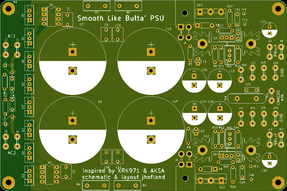
Yes, that’s correct. You can also tell by the pads: square is pin 1(Base).
Hi X,
Sorry - a couple of Qus:
You said "square is pin 1 - the Base ".
Yes, pin 1 is the base for the transistors used at:
* Q10 (2SA1943), and
* Q12 (2SC5200).
However, the pin layout for Q9 (BD139) and Q11 (BD140) have the Emitter as pin 1.
So, Qu 1: does that mean the square pad on the PCB, for these transistors, is:
* pin 1 (which is the Emitter)
* or the square pad is for the Base - as this is the convention jhovland always uses?
Qu 2: I don't know how I did this but for Q10 & Q12, I ordered:
* TTA1943Q & TTC5200Q
* instead of 2SA1943 & 2SC5200.
Are the ones I ordered OK ... or do I need to get 2SA1943 & 2SC5200?
Thanks,
Andy
This is always true on SLB: square pad is pin 1. Pin 1 is left pin when viewed legs down and label/marks visible.
Not all PCBs have a square pad on pin 1 or square pad at all.
The BJTs you got are good. It’s a newer package in TO-247 I think.
Not all PCBs have a square pad on pin 1 or square pad at all.
The BJTs you got are good. It’s a newer package in TO-247 I think.
This is always true on SLB: square pad is pin 1.
Great - thanks, X.
The BJTs you got are good. It’s a newer package in TO-247 I think.
Whew! Thanks. 🙂
Andy
I apologize if this has been answered already - I've read most of the posts, but not all. I know this PS was designed to be used with class A amps, but does the design require a certain amount of constant current draw to work effectively?
I ordered a pair of dual-rail boards and would like to use them with a class A/B chip amp initially, but perhaps a class A amp down the road. If the chip amp current requirements are under 5A, is there any reason why this PS wouldn't work effectively?
I ordered a pair of dual-rail boards and would like to use them with a class A/B chip amp initially, but perhaps a class A amp down the road. If the chip amp current requirements are under 5A, is there any reason why this PS wouldn't work effectively?
I just placed another order for more SLB's as my current inventory has now sold out. So please be patient if you just ordered some. Manufacturing is now 10 days due to Covid19. It used to be 5 days.
Thanks for all the interest in this PSU design!
Thanks for all the interest in this PSU design!

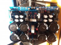

That’s some quick soldering - You are fast TT!

Those were indeed, the final set I had on hand.
Went to breakfast with a friend came back and got to work... it doesn't hurt that those are the 3rd and 4th of the SLBs I have built.
The beer is correct, I been up since about 3:30, so it's just about time for a couple. 🙂
I found a slick way to solder all those STP110N8F6 in place. Just drop them all in and sandwich them in 2 masking tape one side about to the bottom of the sink area and the other over to the board. It pulls them all inward and aligns them perfectly. No soldering one leg and adjusting. I did all those in about 10mins. Just make sure you do them before you put in those big mamajama caps.
Last edited:
Having difficulty in understanding the explanation - could be a little more precise?
I found a slick way to solder all those STP110N8F6 in place. Just drop them all in and sandwich them in 2 masking tape one side about to the bottom of the sink area and the other over to the board. It pulls them all inward and aligns them perfectly. No soldering one leg and adjusting
I found a slick way to solder all those STP110N8F6 in place. Just drop them all in and sandwich them in 2 masking tape one side about to the bottom of the sink area and the other over to the board. It pulls them all inward and aligns them perfectly. No soldering one leg and adjusting
I found a slick way to solder all those STP110N8F6 in place. Just drop them all in and sandwich them in 2 masking tape one side about to the bottom of the sink area and the other over to the board. It pulls them all inward and aligns them perfectly. No soldering one leg and adjusting. I did all those in about 10mins. Just make sure you do them before you put in those big mamajama caps.
Yes, you sure are quick! 🙂
I too - like James - don't get your method? 🙁
But if you proceed as I do - soldering by increasing component height ... you simply put them in place and turn over the PCB. As the STP110N8F6s are the tallest components - at that stage of the build - they get pressed against the board.
Andy
I did it the old fashioned way, one leg first and then adjust before doing the last 2. Takes 15min. The tape idea sounds handy - use blue tape.
Basically one strip on the 8 metal backs align them flat to one another. Another strip from PCB up to bodies on front, aligns them perpendicular to the PCB. Right?
Basically one strip on the 8 metal backs align them flat to one another. Another strip from PCB up to bodies on front, aligns them perpendicular to the PCB. Right?
Group solder
Yes, that's it exactly, stumbled on it and did the centers as you said, but they were all perfect, so I just did one leg on each and moved to the next to prevent heat build-up, when I was done I removed the tape and it's what you see in the picture. No tweaking of any kind... in fact there are a couple not perfect and that was from handling after the fact.
Sorry I didn't get photos, let me tape it off and show, you just remember the large caps are not there...
Okay, here it is quick and dirty, but the extra tape hanging off would be reversed, so it was taped to the PCB where the large caps are... You just take your time when taping, make sure they are all flush and no air gaps in the tape on top.
I did it the old fashioned way, one leg first and then adjust before doing the last 2. Takes 15min. The tape idea sounds handy - use blue tape.
Basically one strip on the 8 metal backs align them flat to one another. Another strip from PCB up to bodies on front, aligns them perpendicular to the PCB. Right?
Yes, that's it exactly, stumbled on it and did the centers as you said, but they were all perfect, so I just did one leg on each and moved to the next to prevent heat build-up, when I was done I removed the tape and it's what you see in the picture. No tweaking of any kind... in fact there are a couple not perfect and that was from handling after the fact.
Sorry I didn't get photos, let me tape it off and show, you just remember the large caps are not there...
Okay, here it is quick and dirty, but the extra tape hanging off would be reversed, so it was taped to the PCB where the large caps are... You just take your time when taping, make sure they are all flush and no air gaps in the tape on top.
Attachments
Last edited:
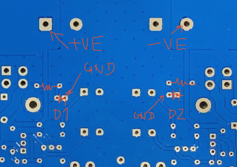
A Qu for anyone who has got a working SLB.
On the dual-rail PCB, D1 & D2 have a square pad in the lower position.
The 'standard' used on the PCB is that the square pad is 'Pin 1'.
Now:
* I would expect that 'Pin 1' would be the Anode
* however, the way the PCB is laid out, I would expect the lower position on both LEDs would be the Cathode.
Can someone tell me the correct orientation, please.
Thanks,
Andy
Hi Andy,
You have the board in front of you and you have the schematic, I assume you also have a continuity checker. Please spend a few minutes studying where the traces go from the pads and you can answer all of these “orientation” questions yourself. It’s good to do this in general. Especially when you wire the flying leads to the BJT. You always have to verify the connection is correct yourself before turning on the power. Silkscreens and their designers can have (and will have) errors. This is the only way to help ensure you don’t see tragically avoidable magic smoke come out when powering up the amp. There’s no harm done with the LEDs as they are indicators only.
So flip the board over and you will see that D1 is the LED for the positive rail cap, that goes to the current limiting resistor then D1. Current flows from positive to negative. The cathode is normally marked with a bar on the diode. It makes sense to mark the cathode with a square pad. No one (except on SMT diodes) marks the anode of a diode. But if in doubt, follow the actual trace of the board in front of you. Look back to the schematic and you will see a correspondence.
Finally, it’s only an indicator. Mount it backwards and it won’t light. You then reverse it.
But spending 5 minutes looking at the board in-hand and comparing with the schematic is always the best way to do it. The same questions about pad 1 pin 1 for the BJT is also answered this way. Look at the supply of voltage upstream and which pin it goes to vs the one downstream. Those will tell you where the collector or emitter are (depending on the +ve or -ve).
Hope this helps.
Attachments
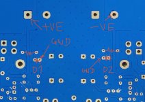
Thank you very much for your detailed explanation, X.
The problem is that I am used to Hugh's PCBs - where the traces are clearly visible ... both on top and undeneath the PCB. But, basically, I couldn't exactly see where the traces go on your PCB ... your drawing on the above pic has helped me do this. 🙂
Andy
The problem is that I am used to Hugh's PCBs - where the traces are clearly visible ... both on top and undeneath the PCB. But, basically, I couldn't exactly see where the traces go on your PCB ... your drawing on the above pic has helped me do this. 🙂
Andy
- Home
- Group Buys
- The SLB (Smooth Like Butter) Active Rect/CRC/Cap Mx Class A Power Supply GB