Thank you Zen Mod but I'm still confused. What is the local loop to which you refer?
Isn't original Schade is an example of common cathode operation (I could easily be wrong here) in which case there is clearly negative feedback. I can see how this works for FETs in common source mode but I don't see how this translates to source follower as per Lynn's circuit.
I suppose if you broaden the definition to be anything that alters the transfer characteristic as you suggest then this could be said to be Schade but personally I would prefer a less confusing term.
I remember Papa saying many time that the transistor doesn't know whether it is in a common source or common drain circuit, it is all a matter of point of reference.
Well this is an unexpected twist or change in direction...
I can see why the two approaches you outline are equivalent but I don't understand why the second is an example of Schade. Isn't Schade a type of feedback? I see only an input attenuator here and no feedback. Am I just being even dumber than usual? Can you explain please?
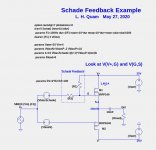
It is a unexpected twist and it is conceivable that there could be a minor modification to the OS circuit. Before ordering PCBs I wanted to better understand the output stage, how I arrived at the design, and how is related to the original FirstWatt SIT-3. I am working on a series of posts about this.
I agree that the transistor doesn't know or care what we call the topology it is used in but the latter certainly does make a difference. Each topology, i.e. common source, gate and drain have different characteristics. Negative feedback is easily understood in common source where the feedback is taken from the output (drain) and is out of phase with the input (gate). However, in a follower there is no signal at the drain to feed back only that of the output at the source which is in phase and of roughly the same magnitude as the input (gate). Sorry to labour the point- I don't really care what we call these things as long as we all have the same understanding. Which brings me back to my original lack of understanding, i.e. from where does the feedback come in a Schaded source follower? I suspect I must be missing the point here...
Anyway, looking forward to your next set of posts Lynn.
Anyway, looking forward to your next set of posts Lynn.
Think of the signal on the drain relative to the gate and the signal on the gate relative to the source. That is the common source perspective of the signals by which we normally view Schade feedback.
Think of the signal on the drain relative to the gate and the signal on the gate relative to the source. That is the common source perspective of the signals by which we normally view Schade feedback.
But the signal on the drain is zero in a source follower isn't it, given that the drain is connected to the supply, i.e. signal earth? The signal at the source is similar to that at the gate due to local feedback from the output load (or degeneration resistor if there is one). How does adding the two Schade resistors before the gate change any of this other than to reduce the output signal by the attenuation factor?
Thanks for you patience and apologies if I am wasting your time Lynn.
Yes, the AC signal on the drain is zero, hence the signal on the drain relative to the gate (Vdg) is -V(gate,0). Likewise the AC signal on the gate relative to the source (Vgs) is definitely not zero. Consider the FET transconductance gm = d(Idrain)/d(Vgs).
Crank up LTSpice and look at the signals: V(D,G) and V(G,S).
Crank up LTSpice and look at the signals: V(D,G) and V(G,S).
I'm beginning to feel like the idiot pupil 🙁
I agree with all you said but I'm missing out on the significance I suppose. Vgs is definitely not zero as you say, but it also does not vary much due to local feedback from the source load. In anything other than a follower this would be different. So, my question remains: what useful effect do the input attenuation resistors (Schade) have on the output other than to reduce it in level? What am I missing here?
I agree with all you said but I'm missing out on the significance I suppose. Vgs is definitely not zero as you say, but it also does not vary much due to local feedback from the source load. In anything other than a follower this would be different. So, my question remains: what useful effect do the input attenuation resistors (Schade) have on the output other than to reduce it in level? What am I missing here?
I'm not very proficient in LTSpice as it is not my simulator of choice. Nonetheless since you have taken the trouble of providing files, I have given it a go.
I see what I expect to see (I think), i.e. small change in Vgs and a much larger change in Vdg with signal. What exactly should I be looking at?
I see what I expect to see (I think), i.e. small change in Vgs and a much larger change in Vdg with signal. What exactly should I be looking at?
two cases:
- Schade alteration of transfer characteristic due to effects in AC domain ( call it feedback; example - Papa's big IXYS Pucks SE amp from BAF2015)
-Schade alteration of transfer characteristic due to effects on part biasing/cunning divider of both AC/DC changes seen by part itself (be clever, make a name)
Attachments

Last edited:
OK, I guess I'll have to try changing the resistor values to see both. A bit beyond my current proficiency with LTSpice so I will try this with my usual simulator.
I must admit I hadn't considered the impact due to biasing although I now see that this could be interesting. Don't much fancy coming up with a name for something I only partially understand. Just call me sissy.
Just looked at the BAF2015 circuit (thanks for the reference) and here, thank goodness, I can both see and understand the Schade feedback as it is applied to a conventional common source stage.
Last edited:
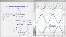
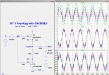
Here is another big surprise. While creating posts showing the relationship between the FirstWatt SIT-3 and the SIT3X I tried a parameter variation with the FirstWatt SIT-3 topology and the 2SK182ES/IXTN40P50P FETs. The result has very good performance with the simplest circuit topology. The only downside vs. the SIT3X is a lower damping factor of 34 vs. 80.
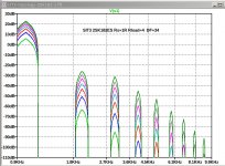
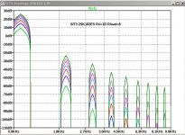
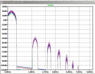
The spectral plots are at 1kHz and 1W, 4W, 9W, 16W, 25W, 36W and 49W. Included below is a standalone LTSpice .asc file for circuit.
The spectral plots are at 1kHz and 1W, 4W, 9W, 16W, 25W, 36W and 49W. Included below is a standalone LTSpice .asc file for circuit.
Attachments
I forgot to mention one other negative about the circuit in the previous post: the output stage power consumption is about 225W vs. about 170W.
But another positive aspect is that there is so much source degeneration of M1 that the optocoupler bias circuit is not needed to maintain bias stability.
But another positive aspect is that there is so much source degeneration of M1 that the optocoupler bias circuit is not needed to maintain bias stability.
Here are some comparisons of the two circuits at 10W output into a variety of loads: 4R, 6R, 8R, 10R, 12R and 16R.
What is interesting is that the SIT3X with the attenuation factor A=0.9 gives totally reversed FET current variations vs Rload compared to the SIT3 topology with the 2SK182ES/IXYS-PFET. When I changed the SIT3X attenuation factor A=0.91 the AC current variation between the FETs was is more balanced.
What is interesting is that the SIT3X with the attenuation factor A=0.9 gives totally reversed FET current variations vs Rload compared to the SIT3 topology with the 2SK182ES/IXYS-PFET. When I changed the SIT3X attenuation factor A=0.91 the AC current variation between the FETs was is more balanced.
Attachments
-
 SIT3-2SK182-Rs1.0-10W-Rload-sweep.jpg527.3 KB · Views: 624
 -
 SIT3X-OS-Perfect-FE-A0.9-10W-Rload-sweep.jpg701.2 KB · Views: 184
 -
 SIT3X-OS-Perfect-FE-A0.91-10W-Rload-sweep.jpg679.5 KB · Views: 173
 -
 SIT3-Rload-sweep-comparison.jpg270.7 KB · Views: 163
 -
 SIT3X-OS-Perfect-FE-A0.91-10W-Rload-sweep-spectra.jpg126.4 KB · Views: 141
Here are some comparisons of the two circuits at 10W output into a variety of loads: 4R, 6R, 8R, 10R, 12R and 16R.
What is interesting is that the SIT3X with the attenuation factor A=0.9 gives totally reversed FET current variations vs Rload compared to the SIT3 topology with the 2SK182ES/IXYS-PFET. When I changed the SIT3X attenuation factor A=0.91 the AC current variation between the FETs was is more balanced.
What is interesting is that the SIT3X with the attenuation factor A=0.9 gives totally reversed FET current variations vs Rload compared to the SIT3 topology with the 2SK182ES/IXYS-PFET. When I changed the SIT3X attenuation factor A=0.91 the AC current variation between the FETs was is more balanced.
What would be the ideal behavior as a function of load?I think you will want to start looking at load dependency.

In a single-ended follower, the SIT would do all of the work, but that requires about 2X bias current for the same max output power. With the SIT3X circuit (Schade feedback on the PFET) the AC current balance between the SIT and the PFET can be adjusted.
What do your ears say?Ideal behavior is the one that the listener likes.
- Home
- Amplifiers
- Pass Labs
- The SIT-3X Amplifier