Will do. Thank you for that. Easy to check and confirm.I would check the bias current of the power Mosftes first.
I can only take a bit of a guess here. Graphs attached for others below. I am trying to remember to standardize my scaling for easier comparisons, but... I'm not quite there yet with "automated scripts". So, that is my fault. If we compare the output at (for example) 1W into 8R for both, they are relatively close at -85dB. I did not take the SE version down to very low output ranges b/c it was more for performance than for diagnostics. The SE version remains relatively flat throughout the entire output range, while the Balanced version has a decline. My guess is that the decline is due to the 2nd cancellation. We can also see that in the FFTs. I'll post some balanced FFTs when I get the one board properly diagnosed and fixed. Those higher % / dB THD+N could be from noise too. The noise is a very high contributor at those low levels due to my unfinished wiring. We will see, but that's my guess for now.f you compare your measurement results from the balanced and the original configuration with a linear PSU (post #400), you'll notice that in the power range up to 1 W there are no improved THD values. The most performance advantage seems to be in the high power range from 1 W upwards.
Why is that the case, even though the even harmonics cancelation?
Thanks!!!

The slope of the curve at power levels below 1 Watt suggests that noise dominates the THD+N measurement in that zone.
The slope of the curve at power levels below 1 Watt suggests that noise dominates the THD+N measurement in that zone.
Holy Moly! I may actually be starting to understand this a little.Those higher % / dB THD+N could be from noise too. The noise is a very high contributor at those low levels due to my unfinished wiring.
Thank you for confirming @Marcus Halberstram Much appreciated.

The THD differences you show could be dominated by the second harmonic (H2) due to differences in the FET transconductances.
Are the FETs for the left and right channels the same? Are they the "matched" pairs that I distributed with the PCBs?
Do you have THD vs. Watts curves for left and right channels?
Are the FETs for the left and right channels the same? Are they the "matched" pairs that I distributed with the PCBs?
Do you have THD vs. Watts curves for left and right channels?
I did some very crude checks. Even though I goofed up a board with bad measurement technique (and worse yet, I know better / it's in my procedure how to do it properly)... it's a good learning. At least I was smart enough to not hook it up to speakers until I completely verify that it's fixed and working properly.I would check the bias current of the power Mosftes first.
See below:
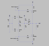
Voltage across sense resistors (bias current indicator) - 122.5mV
DC offset of sole board (from GND to out of individual board) - 4V1 😱 Previously was below 2mV if I recall. Can't lower to below 3V2 with pot. Clearly one MOSFET isn't "pulling its weight".
For PFET:
GD - 15V6
GS - 4V1
DS - 19V7
For NFET:
GD - 17V4
GS - 4V2
DS - 21V6
It may be clearly obvious to someone that knows ... but I wish I knew exactly what this indicated. Is it wise to put a scope across GND to the source of each output MOSFET to see which one (or both) may be acting up, or is the issue abundantly clear to someone that understands this better than I?
Suggested next steps are appreciated with my gratitude in advance. Blindly replacing parts isn't my idea of how to learn.
Last edited:
Makes perfect sense, but I am not sure.The THD differences you show could be dominated by the second harmonic (H2) due to differences in the FET transconductances.
I am not sure what you're asking re: "same". Yes, they're the ones you sent.Are the FETs for the left and right channels the same? Are they the "matched" pairs that I distributed with the PCBs?
For the SE I did previously with the linear PSU? I do not, but I can do them for each of the individual 4 boards once I get the board I've goofed up fixed properly. That may be informative and fun.Do you have THD vs. Watts curves for left and right channels?
Thank you!

Again, I know this isn't a thread to teach Patrick the basics, but ... all help is appreciated.For PFET:
GD - 15V6
GS - 4V1
DS - 19V7
For NFET:
GD - 17V4
GS - 4V2
DS - 21V6
When in doubt, I look at the schematic and compare to a known-working-good board.
For a known good board -
For PFET
GD - 16V6
GS - 4V1
DS - 20V7
For NFET:
GD - 16V2
GS - 4V3
DS - 20V5
The good board and the bad board share the same PSU / same rails.
Edited for clarity - These two boards are on the same channel. The "bad" board is set up for positive phase amplification, and the "good" board is set up for negative / inverted phase amplification.
Last edited:
For those looking for additional FETs: The Build Guide mentions alternate FETs.
Probably the best alternate FETs at this time are the IXYS IXTQ36N30P and IXTQ36P15P.
Probably the best alternate FETs at this time are the IXYS IXTQ36N30P and IXTQ36P15P.
I like that approach... I was going to do it, and I'm willing to do it, but it's going to tell me one of two things...Try swapping the FETs between boards. (Easy is the FETs are socketed, but harder if soldered).
1) Issue is MOSFETs (problem moves with MOSFETs).
2) Issue is something else (problem stays with board).
If it's #2... further diagnosis will be in order.
I was hoping to narrow it down before taking two boards out of commission. (They're not socketed, but I'm handy with a de-soldering gun).
Off to the bench.
Does it matter if they are different manufacturers? Say IXYS vs Littlefuse?Probably the best alternate FETs at this time are the IXYS IXTQ36N30P and IXTQ36P15P
Apparently IXYS was acquired by Littelfuse...
https://www.littelfuse.com/about-us...littelfuse-completes-acquisition-of-ixys.aspx
https://www.littelfuse.com/about-us...littelfuse-completes-acquisition-of-ixys.aspx
Will do.Ad. 2) Check the offset at FEOut
Suspect board has already been removed from chassis / PSU. Removed MOSFETs from board. Checked with the El-cheapo Mega tester along with a quick resistance check against known good MOSFETs. They seem to be in range with no obvious damage.
I'll install them on the other known-good board. If problem follows the MOSFETs, then I'll replace the MOSFETs.
If problem doesn't follow the MOSFETs, then next step will be to check above on the "bad" board. I'll install the board on a test bed with PSU / heatsinks and do further checks.
Have to pause for the day, but I'll be back at it tomorrow.
Thanks to you, Lynn, and to all the others that offer their expert advice. I'll get it back up and running properly. It's become a challenge now...plus it sounded mighty fine before I messed it up.
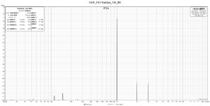
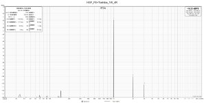
I ran some new spectral measurements using FQA28N15 paired with IXTQ36P15P FETs. Both of these FETs are currently available at Mouser.com (1000s available). The HGF was configured at 28V rails, 1.3A bias, 12dB global feedback.
The IXTQ36P15P appears to nearly identical to the FQA36P15 which is not available.
Here are some distortion vs. watts sweeps for the left and right channels for 8R and 4R loads:

The IXTQ36P15P appears to nearly identical to the FQA36P15 which is not available.
Here are some distortion vs. watts sweeps for the left and right channels for 8R and 4R loads:
When I had my new FE on the workbench, I immediately had the opportunity to test the Toshiba power MOSFETs 2SK3497/2SJ618, which were actually intended for the M2OPS. So far there has been no answer as to how they will behave in HGF.
Fortunately, I was able to determine that the bias remains very stable. Adjusting went without any problems. The bias circuit resistors were the same as with Fairchild parts.
It is very interesting that with this FE and an NFB of only 25 dB the DF is at 350. Looks promising...
Fortunately, I was able to determine that the bias remains very stable. Adjusting went without any problems. The bias circuit resistors were the same as with Fairchild parts.
It is very interesting that with this FE and an NFB of only 25 dB the DF is at 350. Looks promising...
Attachments
https://www.diyaudio.com/community/threads/complementary-power-mosfets.378024/post-6889027

That measurement from Twitchie is M2OPS alone.
In open loop, no NFB.
Patrick
That measurement from Twitchie is M2OPS alone.
In open loop, no NFB.
Patrick
My build progress so far. Planning to use a single 0.1R/5W KOA BPA resistor instead of using couple of 0.22R/1W per the BOM as I do have lots of BPR resistors. Used sockets to mount R11/12 with 15k resistors temporarily.

A major reason that current sense resistors R1 and R2 are pairs of 0R22 resistors rather than singles is to distribute the current to multiple pads. Although the idle bias current is only around 1.3A, the peak current can easily reach 5A for 20V peak output into a 4R load (50W rms).
Hmm so you suggest better to use pair of either 1W or 2W resistors of 0.22R rather than using a single 0.1R/5w resistor. Let me get these ordered from Amazon the metal film ones rather than carbon or metal oxide.
Edit: @lhquam sorry I think I missed some of your text that you quoted earlier when we got the PCBs along with matched FETs. There are 2 sets of 4 transistors each marked with numbers, not sure which of the 4 are matched and the other might be extra transistors which were offered by you.
Thanks
Edit: @lhquam sorry I think I missed some of your text that you quoted earlier when we got the PCBs along with matched FETs. There are 2 sets of 4 transistors each marked with numbers, not sure which of the 4 are matched and the other might be extra transistors which were offered by you.
Thanks
Last edited:
- Home
- Amplifiers
- Pass Labs
- The Holy Grail Follower Output Stage


