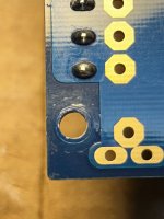
@ACnotDC - Thank you! That is very kind. re: the GND connections. I fully admit that I am a novice in this area. I had (using those boards) the GND connected both "at the back" in the AKA 'dirty' area and also at the front (where it is now) in the 'clean' section. A kind user pointed out to me that currents aren't equal all over the same pad / plane and that yes, those two segments / areas behaved differently in terms of noise. So, I removed all the connections in the "dirty" section. I think that's what Tungsten may have observed in the photos, the 'shiny' pads from the remaining solder left after removal.
However, your point is taken, and I can "beef up" that one section / area easily. I will do it. I had left the other holes empty b/c I thought... I might use them for spade connections, but I've since abandoned that idea.
I appreciate the kind words and ideas to improve/learn as always.
However, your point is taken, and I can "beef up" that one section / area easily. I will do it. I had left the other holes empty b/c I thought... I might use them for spade connections, but I've since abandoned that idea.
I appreciate the kind words and ideas to improve/learn as always.
No, the P1 potentiometer is adjusted for minimum (zero) output offset. That and the global negative feedback loop compensates for FET Vgs threshold mismatch.Does this bias technique in general require matched thresholds (absolute value) of the P and N MOSFETS?
Thanks! Would be useful to add this link to the first post of the thread to make the Build Guide easy to find.
IAIMH - I'm totally in line with ACnotDC's suggestion there. You really want low impedance between the caps on each side, the lower the better. I have been adding a heavy gauge copper wire / rod to the pcb between the caps, from terminal to terminal, "beefing up" as you say. There are big current pulses flowing there, and that new lower impedance at a critical spot helps me sleep at night..
A low impedance connection between the two PS grounds certainly will not hurt, but if you carefully examine where the large currents flow it is not between the two PS grounds but through the output FETs and the output load (speaker).
From a ground loop perspective, it would be better to separate the two grounds, essentially creating two "mono-block" channels. Eliminate the ground loop breaker on whichever PCB uses it, and connect a thermistor from each PS ground to the chassis.
From a ground loop perspective, it would be better to separate the two grounds, essentially creating two "mono-block" channels. Eliminate the ground loop breaker on whichever PCB uses it, and connect a thermistor from each PS ground to the chassis.
While that is a reasonable suggestion, the “Universal PS“ board does not support that level of separation.
Speaking of output FETs, that's another place I like to beef up sometimes. That mile long trace on a pcb between source pins.... I like some more copper there too. Fortunately lhquam is no dummy and we get a parallel run top and bottom on these HG boards.... nice.
Any updates on this?For any of you thinking about doing your own PCB layout, I have a minor addition your might want to include.
For each output FET, provide for the possible addition of a resistor from gate to source. This will allow you to reduce the gm of that FET resulting in the modification of the 2nd harmonic level.
I will post some simulations showing the effect.
Thanks,
There is global negative feedback through resistor RF4 into the front-end opamp and DC coupked through the wiper of P1. This helps to stabilize the DC offset.
I must retract all of the erroneous comments about that power supply. I didn't look carefully enough at that PS schematic and thought it was something else. My bad.It appears that your PS has two totally separate diode bridges and CRC filters, as with mono blocks.
This is a case I did not discuss in the Build Guide. Try eliminating the ground loop breaker by connecting the RCA GND and In- to (PCB) GND as it is with the channel. And each PS GND should have a thermistor to chassis GND.
ACnotDC in post #419 is correct about tying the two PS grounds together, because there is a high current path between those grounds.
ItsAllInMyHead you should connect the ground wires to the ZD25-Mini PCBs to the same PS GND point to form a star ground. The image in post #407 shows one ground on the PS+ GND side, and the other on the PS- GND side. Continue to have one ZD25-Min i PCB with a ground loop breaker.
Currently I have too many different projects going and haven't had to time to bench test the modification. But I will sketch it out.Any updates on this?
Thanks,
In a Nelson Pass that I cannot find, he described a trick to lower the gm of a FET using a voltage divider formed by the gate stopper and a resistor from gate to source. This makes it possible to lower the gm without using a source resistor, of course still requires that the the FET bias current is controlled in some manner.
This makes it possible to reemphasize the role of gm in matching the NFET to the PFET and concentrate on a different parameter(s).
Those Gerber files in post #212 are corrected for the PCB layout error.
No modification is needed.
No modification is needed.
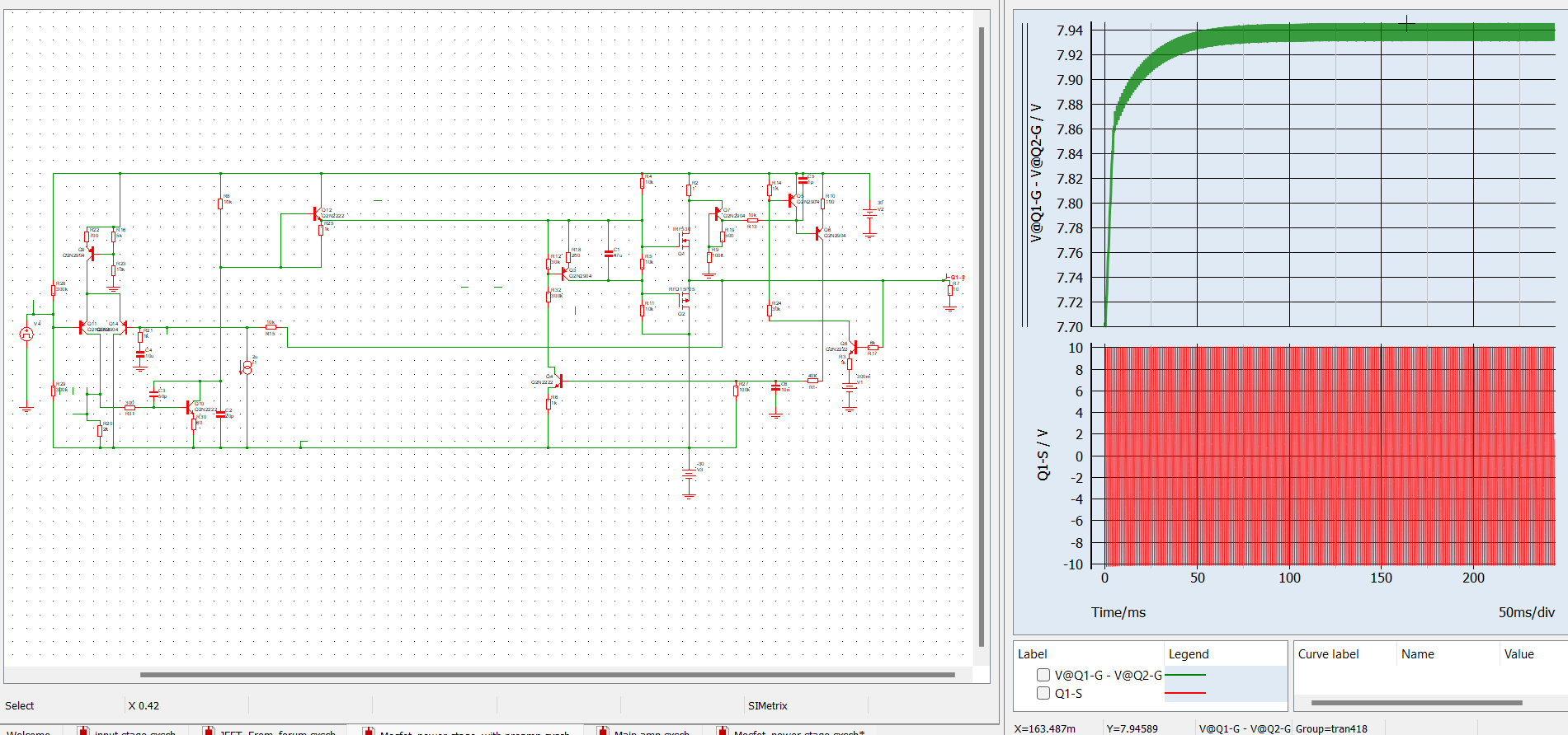
Sensing MOSFET bias during off-cycle of N MOSFET and integrating in dedicated feedback loop . Controls bias to 20mA. Including preamp stage this time
Green trace is differential bias voltage between gates.

Green trace is differential bias voltage between gates.
Not a worry. For all intents and purposes, those two connection points are "the same". You are correct that one channel's GND was connected to the + rail side of the PSU and one to the - rail side of the PSU. However, they did have a jumper between to "make" it a bipolar supply with a common GND.I must retract all of the erroneous comments about that power supply. I didn't look carefully enough at that PS schematic and thought it was something else. My bad.
ACnotDC in post #419 is correct about tying the two PS grounds together, because there is a high current path between those grounds.
ItsAllInMyHead you should connect the ground wires to the ZD25-Mini PCBs to the same PS GND point to form a star ground. The image in post #407 shows one ground on the PS+ GND side, and the other on the PS- GND side. Continue to have one ZD25-Min i PCB with a ground loop breaker.
I'm never embarrassed to share mistakes in the hopes that someone reading may not replicate my error ... OK, I'm a little embarrassed.
I took out the PSU yesterday just after William's post. I added additional jumpers between the GND points from the "+" rail side to the "-" rail side of the PSU board per everyone's kind suggestions. I thought it would be also be a wonderful time to redo the layout a little to add some physical space between the DC wiring and the PEM.
Well .... I have now joined the "You can't fix stupid" club.
My intention was to "go vertical" and move the PSU board toward the front of the chassis. It was mounted on threaded rods to raise it over the toroid. I've mounted things similarly before with another PSU. I put a set of cap boards over the inductors/chokes in a "CLC".
I was in a hurry (stupid) and didn't check the clearances. My K-lock nut on the underside of the board was large enough to overlap slightly with one (or both) of the supply traces/pours. Additionally, I had tightened it enough to where it cut through the solder mask and shorted one of the rails to chassis GND through my mounting rod.

I typically have these boards mounted with nylon spacers.
I was
 at my boneheadedness and decided to leave it alone for the rest of the day.
Thankfully, I was at least smart enough to re-check the PSU with a variable transformer before re-connecting the amp boards. I didn't however have it on a DBT and wasn't using a 0A5 fuse per my normal process. It was at about 40VAC at the primaries when it when poof. So, at the moment, I am trying to figure out which component(s) released that little puff of smoke. Troubleshooting is not my strong suit...
So, if anyone has a tip for boneheads, I'm all ears. I had mentioned wanted to use a different PSU anyway.

So, I'm putting together another PSU in the interim, until I decide what to use permanently.
Moral of the story... don't be a doofus like me.
Last edited:
I have done similar things. One common failure is blown resistors in the CRC filter. Check them first. Look for discoloration. Put an ohmmeter across them. Most multimeters cannot accurately measure below 1 ohm, but you can tell if the resistors are totally blown.
Another possibility is blown rectifiers.
Another possibility is blown rectifiers.
- Home
- Amplifiers
- Pass Labs
- The Holy Grail Follower Output Stage