The build guide is very well written. I appreciate the explanations of how the different circuit options work. It is clear that this is a project that may be enjoyed by intermediate to advanced builders. There are a lot of things that I look forward to trying.
The option to use larger “hockey puck” FETs is one that will be explored in a much larger chassis.
The option to use larger “hockey puck” FETs is one that will be explored in a much larger chassis.
I wonder about the need for hocky pucks. If you continue to use the opa151 the rail voltages are limited to +/-30V and the max output power into 8 Ohms will be about 50W (voltage swing of +/-28.3V). That requires a maximum of 3.54A current.
Where the pucks might be needed is with lower impedance speaker loads. At 4 Ohms you might get 100W output with 7.1A max current. Look at the SOA plots for the various transistor options.
Where the pucks might be needed is with lower impedance speaker loads. At 4 Ohms you might get 100W output with 7.1A max current. Look at the SOA plots for the various transistor options.

I would switch to the OPA445 to allow higher rail voltage in the hockey puck version. I already have a few on hand following my experiments with various DIY Sony VFET front ends. They sound much like the OPA551.
Operating the output FETs in their sweet spot is more of a design consideration than achieving a specific power output with the speakers.
Operating the output FETs in their sweet spot is more of a design consideration than achieving a specific power output with the speakers.
Hi @lhquam
Thanks a lot for the build guide.
Thanks also for making us aware of the Meanwell N2 series. I just knew about the standard (older) type. N2 is the same price so a bonus. Here is a copy paste from Meanwell talking about the difference between the 200W smps.
“Featuring LRS-N2 Series
The enclosed-type is one of the major product lines, MEAN WELL also continues to develop new products to provide more standardized power supplies to serve global customers and various industrial applications. The biggest difference between the newly-launched LRS-100/200/350/600 N2 series and the previous LRS is providing instant 200% peak power for up to 5 seconds, which reduces the issues when matching with various instantaneous high current during startup applications. Customers don't need to buy higher wattage, simply use it with a normal wattage that combined with instantaneous peak power.”
BR,
Eric
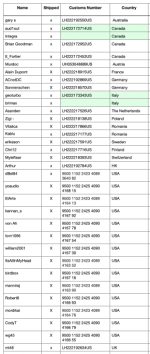
Wonderful, great job!The Build Guide and BOM are here. Attached are two files: Build-Guide.pdf and Build-guide.zip. Build-guide.zip contains test file versions of the BOMs and more detailed versions of the images shown in the pdf file.
First page of Buil.d.Guide.pdf:
View attachment 1292153
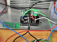
@lhquam - a couple of minor points on the front end schematic and BOM.
For resistor RF2, the schematic shows 42.9K and the BOM shows 43.2K - which is correct?
For resistor RF3, the schematic shows 518K and the BOM shows 511K - only small differences, but we might as well buy the correct values here.
Looking at the photo of the loaded pcb, it looks like the BOM has the correct values for these 2 resistors.
Everything else seems to agree between the schematic and BOM.
Thanks..
Last edited:
Use the values in the BOM. I just finished building and tested another pair of boards with the parts in the BOM, without the optional parts. I actually did the Mouser cut and past BOM entry to order the parts.
I installed the boards into a 4U Store chassis that previously had F7 boards and a +/-25V linear supply. It runs just fine.
I installed the boards into a 4U Store chassis that previously had F7 boards and a +/-25V linear supply. It runs just fine.


All that snow must have melted in the Midwest. Postal Service can finally put the pedal to the metal.
For any of you thinking about doing your own PCB layout, I have a minor addition your might want to include.
For each output FET, provide for the possible addition of a resistor from gate to source. This will allow you to reduce the gm of that FET resulting in the modification of the 2nd harmonic level.
I will post some simulations showing the effect.
For each output FET, provide for the possible addition of a resistor from gate to source. This will allow you to reduce the gm of that FET resulting in the modification of the 2nd harmonic level.
I will post some simulations showing the effect.
^ Thanks again for a great project, Lynn. With provisions for above and all the options in the guide, this could provide a lot of fun and learning.
In addition, thank you for the extra FETs. Could you provide some insight re: which ones are the ones to use vs. the extras. I could not make heads or tails of the markings. I read the guide and previous posts, so if I've missed it somewhere, my apologies.

Patrick
In addition, thank you for the extra FETs. Could you provide some insight re: which ones are the ones to use vs. the extras. I could not make heads or tails of the markings. I read the guide and previous posts, so if I've missed it somewhere, my apologies.
Patrick

I should have explained that earlier.
- The extra FETs are marked with X on the backside.
- The markings on the tops of the FETs to associate measurements to FETs, and ultimately for the sorting process.
- The little PCB is for an optional star ground. With the F5m was was useful in reducing power supply induced noise in the grounding. For the ZD25-Mini, the ground-loop breaker and differential inputs to the fount end seem to be more effective at reducing the noise issues. The worst audible noise I have encountered without either the star ground or ground-loop breaker has been a faint buzzing with my ear about 2 inches from the speaker cone.
Attachments
- Home
- Amplifiers
- Pass Labs
- The Holy Grail Follower Output Stage