www.patent2pdf.com
type in the patent number and retrieve it.
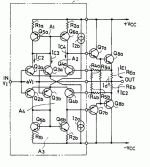
Pioneer patent is elegant and robust, can be found in their commercial products, however this topology is native to Single ended push pull scheme, i.e. something like ''Krill'' input diamond.
type in the patent number and retrieve it.
Pioneer patent is elegant and robust, can be found in their commercial products, however this topology is native to Single ended push pull scheme, i.e. something like ''Krill'' input diamond.
OS, precisely yes.
This topology is based on non-linear current mirrors and SEPP. Like most of the non-linear current mirror based solution this one is meant to be immune to teperature co-efficient (in theory).
Wish to simulate?
Cheers.
This topology is based on non-linear current mirrors and SEPP. Like most of the non-linear current mirror based solution this one is meant to be immune to teperature co-efficient (in theory).
Wish to simulate?
Cheers.
This paper explains the working principle of non-linear current mirror based non-switching class-b amp by Prof MJ Hawksford:
http://www.essex.ac.uk/DCES/research/audio_lab/malcolmspubdocs/C82 Non-switching amplifier.pdf
Worthwhile to simulate? Pls notice the references cited in the paper and the relative limitations of known non-switching schemes e.g. Blomely, Tanaka.
Cheers
http://www.essex.ac.uk/DCES/research/audio_lab/malcolmspubdocs/C82 Non-switching amplifier.pdf
Worthwhile to simulate? Pls notice the references cited in the paper and the relative limitations of known non-switching schemes e.g. Blomely, Tanaka.
Cheers
atiq19 said:This paper explains the working principle of non-linear current mirror based non-switching class-b amp by Prof MJ Hawksford:
http://www.essex.ac.uk/DCES/research/audio_lab/malcolmspubdocs/C82 Non-switching amplifier.pdf
Worthwhile to simulate? Pls notice the references cited in the paper and the relative limitations of known non-switching schemes e.g. Blomely, Tanaka.
Cheers
Thank you for that link. It seems to be a fairly complicated way of doing something that can be done more simply.
The earliest of the references listed indicates that someone else was working on this concept at the same time as me. Since we solved the problem in radically different ways, I think it is safe to say that neither of us "borrowed" from the other. I spent a lot of time researching this concept before I claimed it as my own. I think I can stick to that claim. I am referring only to the solution I arrived at of course.
Steve,
I quite like your ingenious piece of works-'krill the little amp that might change your...'. Simple, elegant and proven are 3 words for your design.
I find it overwhelming the human quest for 'applied' science. Equally this applies to other branches of science where several people came up with similar ideas at the same period in different parts of the world.Despite the fact that they never met or spoken to. Perhaps we as a human being share our intuition in parallel world where we interact and overlap.
Things get complicated when comes the commercial arena, for example patent in new electronics invention (?) and circuit topologies. These days you would probably see handful of patents for similar concepts (its all about N-P junctions and possible permutations and combinations of basic elements of electronics 😀 ). Someone once joked (perhaps out of frustration), ''what about patenting a piece of wire?''. Whilist I don't see any problem in doing that I recognise the limitations of modern Hi-fi world R&D's achievements since the invention of solid state diode in 50s.
Cheers
Atiq
OS,
An extension of Hawksford proposal on error correcting non-switching class-B could be and implementation of Technics diode based non-switching O/P stage with 'Kulish corrector' , a concept developed by Mikhail Kulish for error correction. Although in sim, in some instances a 150dB of thd reduction has been reported at full power o/p.
Cheers
Atiq
Attachments
anyone wish to pursue 'Kulish Corrector' concept (in LTP, VAS, EF, CFP) further may see:
http://www.diyaudio.com/forums/showthread.php?s=&threadid=114249&perpage=25&pagenumber=4
http://www.diyaudio.com/forums/showthread.php?s=&threadid=114249&perpage=25&pagenumber=4
One thing I should mention about prof MOJ Hawksford is that he never patented (but someone else later patented his cocept in lieu of him),
1. Error correction topology, perhaps one of the most original topologies proposed in late 70s. (I heard people saying Halcro patented error correction without refering to his works?)
2. Cascoding of BJT stages (Hawksford cascoding, recently re-surrected in some of our DIY threads e.g YAP thread)
3. Non-linear current mirror based VCVS for Output stage topology.
by steve dunlap - Thank you for that link. It seems to be a fairly complicated way of doing something that can be done more simply.
Yes, it is looking more and more like the krill is the simple
way out of the switching dilemma.
OS
Back at it, after playing around with everything, the advice I
received a long time ago " refine what you have" seems to
be the best..

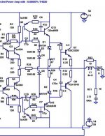
Yes, a triple.. (it was harder to make stable,but worth it)
1. Input stage/CCS - the same as all the other FA's ,but at
4 months and running in the real world , I see no reason
to fix something that is not broken. R6/7/8 can be scaled
for between 40 and 80V rails and all other active components
are up to the job (well derated). I strived to "keep it simple"
by omitting the CM and making up the difference with degen
and high gain group KSC1845's.
2 . Holman /APT " level splitter" - Q4 /5 and 6 are a wilson CM
used to generate a negative "clone" of the top VAS drive.
It is markedly faster than a standard CM used in the FA3
and more accurate too. R14 (VR "BX") can be adjusted to
balance the LPT within .001 mA regardless of amplitude.
This might make the offset trim redundant but I'll get to that
when these are constructed.

3. VAS - standard KSA1381/KSC3503 (Q7/8), no EF needed..
especially now as the triple EF OP places no load on anything 😀
I played with currents ranging from 3mA to 10mA and found
THD20 was best at 6ma (small heatsink )
)
4. - VBE multiplier - here is one aspect that will need input
and or real world testing. I chose diodes to eliminate parasitics
and give me more options (3 or 4 diodes /MUR's- 914's..etc.)
A "leap of faith" in professor leach is in order as I have not
built a triple YET.
5. - The triple... yes, "the leap of faith" I had this part of the
amp oscillate in every way imaginable. With base stoppers at
the outputs it would work with a sine input , but oscillate
with SW input. Another set of base stoppers between
predrivers and drivers would tame it further (tiny bursts at
clipping) BUT C9 and 10 really did the trick (I saw this technique
in many commercial amps). Doing tests with different
C9/10 values showed little effect in regard to OLG or unity gain
so these commercial designers must have it right.. 🙂
6. Simulation performance - This is what left me scratching my
head and wondering why I hadn't persued this route earlier.
I actually got -110DB H2's with traces of H3 only at full power.😎 . At moderate power and 20k almost NOTHING..

I did a MOSFET version and it did as good or better than
the BJT..(attached)
The .ASC's of these amps (FA2T and FA2BST "beast") are
in :http://71.203.210.93/pdf1/Electronics/Projects/Audio_amp/Frugalamp/
"FA2 " folder .. boards will follow .I have not built in a while , but now have a laser printer (MJL quality boards) and need a
"beast" (fa2bst) for my sub and 2 "pretty" amps (fa2t)to show off..
OS
received a long time ago " refine what you have" seems to
be the best..
Yes, a triple.. (it was harder to make stable,but worth it)
1. Input stage/CCS - the same as all the other FA's ,but at
4 months and running in the real world , I see no reason
to fix something that is not broken. R6/7/8 can be scaled
for between 40 and 80V rails and all other active components
are up to the job (well derated). I strived to "keep it simple"
by omitting the CM and making up the difference with degen
and high gain group KSC1845's.
2 . Holman /APT " level splitter" - Q4 /5 and 6 are a wilson CM
used to generate a negative "clone" of the top VAS drive.
It is markedly faster than a standard CM used in the FA3
and more accurate too. R14 (VR "BX") can be adjusted to
balance the LPT within .001 mA regardless of amplitude.
This might make the offset trim redundant but I'll get to that
when these are constructed.
3. VAS - standard KSA1381/KSC3503 (Q7/8), no EF needed..
especially now as the triple EF OP places no load on anything 😀
I played with currents ranging from 3mA to 10mA and found
THD20 was best at 6ma (small heatsink
)4. - VBE multiplier - here is one aspect that will need input
and or real world testing. I chose diodes to eliminate parasitics
and give me more options (3 or 4 diodes /MUR's- 914's..etc.)
A "leap of faith" in professor leach is in order as I have not
built a triple YET.
5. - The triple... yes, "the leap of faith" I had this part of the
amp oscillate in every way imaginable. With base stoppers at
the outputs it would work with a sine input , but oscillate
with SW input. Another set of base stoppers between
predrivers and drivers would tame it further (tiny bursts at
clipping) BUT C9 and 10 really did the trick (I saw this technique
in many commercial amps). Doing tests with different
C9/10 values showed little effect in regard to OLG or unity gain
so these commercial designers must have it right.. 🙂
6. Simulation performance - This is what left me scratching my
head and wondering why I hadn't persued this route earlier.
I actually got -110DB H2's with traces of H3 only at full power.😎 . At moderate power and 20k almost NOTHING..
I did a MOSFET version and it did as good or better than
the BJT..(attached)
The .ASC's of these amps (FA2T and FA2BST "beast") are
in :http://71.203.210.93/pdf1/Electronics/Projects/Audio_amp/Frugalamp/
"FA2 " folder .. boards will follow .I have not built in a while , but now have a laser printer (MJL quality boards) and need a
"beast" (fa2bst) for my sub and 2 "pretty" amps (fa2t)to show off..
OS
Attachments
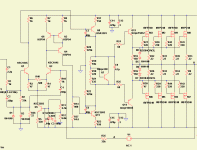
Try KSA1381/KSC3503 for the predrivers too. This is more like the original Leach, where the predrivers and VAS devices are the same.
The Leach is quite stable but then again, he is using pretty old output devices that only have an fT of 4MHz iirc. Jens Rasmussen of Delta Audio has a modern up-to-date version with fast output devices on his site.
http://delta-audio.com/Leach-Clone.htm
The split feedback thing on the original amp is interesting. It may be worth trying this in the sim and seeing what happens.
your fa2-t look's like my v4.1 😀
I'm curious if i try the clone on the top Vas.
I'm listening about 2 weeks this version and I'm joy 😀 .Unlike fa2 I don't have "negative "clone" of the top VAS drive" .
My test say :
slew rate >100v/uS
thd(5khz) =0.0001 %
phase reserve ~ 70degrees.good stability .
I'm curious if i try the clone on the top Vas.
I'm listening about 2 weeks this version and I'm joy 😀 .Unlike fa2 I don't have "negative "clone" of the top VAS drive" .
My test say :
slew rate >100v/uS
thd(5khz) =0.0001 %
phase reserve ~ 70degrees.good stability .
Attachments
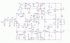
Hi Cat,
C51 is far too small.
It must be greater than or equal to 215uF. Use 220uF
C51>=R3 * C16 *1.414 / R39.
330uF or 470uF would do no harm.
Try adding a big polypropylene in parallel with the electrolytic.
The 1k6 between the pre-drivers limits the current to ~{0.8mA + the driver base current}.
Is that optimum?
The current is optimum(1ma).at that value the noise is good.
Please argument your value of the capacitor analytically ;exactly with the frequency of the pole and zero 🙂
Please argument your value of the capacitor analytically ;exactly with the frequency of the pole and zero 🙂
my argument
I say wat I know 😀
The frequency where it will be an 0 in the feedback network will be f=1/(2*pi*r*c)=0.16/680*47u=5hz (-3db).This 0 will be an pole in the transfer function of the clossed loop of the amp .Do you think that 5 hz it isn't enough 🙂 ?
On the other hand an 0 in the feedback will be at 1/(2*pi*r*c)=0.16/22k*47u=~1hz (here will be an pole in the feedback network and an zero in the amps transfer function(gain)) .So I still think that the 47u cap is very good choice.
Please explain your opinion .
Attachments
Re: my argument
Not 0,my mistake .Pole is what I want to say (attenuation with -3db and -45 degreees in phase)catalin said:I say wat I know 😀
On the other hand an 0 .
let's suppose that the input high pass filter (DC blocking capacitor) removes all the audio signal from the source.
In that situation what will be the Audio frequency voltage across the NFB DC blocking cap. It must be zero Vac.
Let some audio signal pass that input filter.
If the Input filter is set to High Pass ~ 100Hz then what will be the > 150Hz AC voltage across the NFB capacitor if it's impedance at 5Hz matches the feedback lower leg resistor?
Now delete the input filter and pass all frequencies to the amplifier.
What is the AC voltage across the NFB capacitor?
Ah, there is some AC voltage and if DC were present in the input signal there will also be DC across the NFB cap.
Q.) How can we minimise the AC voltage across the NFB cap?
A.) By ensuring that the Input high pass filter attenuates the LF signals to a level, that in comparison the the NFB filter, such that the NFB cap can never develop a significant AC voltage across it.
That requirement of minimising the AC voltage across the NFB cap demands that the Input filter must set the LF bandwidth of the amplifier.
Look at what you have.
The Input filter is set by 4u7F and 22k (RC=103ms) and has F-3dB~1.5Hz.
The NFB filter is set by 22uF and 680r (RC=15ms) and has F-3dB ~11Hz.
Send a signal that has AC content between 1.5Hz and 11Hz. Will there be any AC voltage across the NFB capacitor? Yes.
Now set the NFB filter to input filter F-3dB/1.4 i.e. 1Hz.
Now calculate what AC voltage you can get across the NFB capacitor for signals in the range 0.1Hz to 20Hz. Are any significant? Will these AC voltages give rise to excessive amplifier distortion?
I can't do the sums.
I can see the logic to why the input filter (wherever it is located) must set the bandwidth of the amplifier and why the NFB DC blocking cap must not be used to limit the bandwidth of the amplifier.
Any questions?
AndrewT said:let's suppose that the input high pass filter (DC blocking capacitor) removes all the audio signal from the source.
In that situation what will be the Audio frequency voltage across the NFB DC blocking cap. It must be zero Vac.
Let some audio signal pass that input filter.
If the Input filter is set to High Pass ~ 100Hz then what will be the > 150Hz AC voltage across the NFB capacitor if it's impedance at 5Hz matches the feedback lower leg resistor?
Now delete the input filter and pass all frequencies to the amplifier.
What is the AC voltage across the NFB capacitor?
Ah, there is some AC voltage and if DC were present in the input signal there will also be DC across the NFB cap.
Q.) How can we minimise the AC voltage across the NFB cap?
A.) By ensuring that the Input high pass filter attenuates the LF signals to a level, that in comparison the the NFB filter, such that the NFB cap can never develop a significant AC voltage across it.
That requirement of minimising the AC voltage across the NFB cap demands that the Input filter must set the LF bandwidth of the amplifier.
Look at what you have.
The Input filter is set by 4u7F and 22k (RC=103ms) and has F-3dB~1.5Hz.
The NFB filter is set by 22uF and 680r (RC=15ms) and has F-3dB ~11Hz.
Send a signal that has AC content between 1.5Hz and 11Hz. Will there be any AC voltage across the NFB capacitor? Yes.
Now set the NFB filter to input filter F-3dB/1.4 i.e. 1Hz.
Now calculate what AC voltage you can get across the NFB capacitor for signals in the range 0.1Hz to 20Hz. Are any significant? Will these AC voltages give rise to excessive amplifier distortion?
I can't do the sums.
I can see the logic to why the input filter (wherever it is located) must set the bandwidth of the amplifier and why the NFB DC blocking cap must not be used to limit the bandwidth of the amplifier.
Any questions?
Yes they are 🙂
You say that in the amp will enter very low frequency (1-10hz) and that will be the cause of the noise .From where do you get so low frequnecies
 ?
?Please argument what you say a little mathematical to understand all the people .
My capacitor it is 47u not 22u so I have a pole at 5hz .I understand what you say but ..
So my question is where do you obtain so low frequency (in my case 1-5hz! )
Thank you
- Status
- Not open for further replies.
- Home
- Amplifiers
- Solid State
- The Frugalamp by OS