jkeny said:Andy, I saw these Bob Cordell comments & asked the question what is the relative importance of dynamic Vs Static Xover distortion but got no answer from him. So is static distort ~0.1% or 20% of total Xover distortion?
It depends on frequency, the fT of the output devices, and the drive circuitry. It's important for the drive circuitry to be able to turn off the inactive device as quickly as possible. That's the reason for the cap between driver emitters. If you try full power and increase the frequency enough (say 200 kHz or so, or above), the inactive device will fail to turn off, resulting in common-mode conduction, resulting in smoke.
I'll go out on a limb here and say that given fast output devices (like MJL3281, MJL1302), proper driver design, and signals 20 kHz and below, that dynamic crossover distortion can be mostly neglected. If you have good device models (and that's a big "if"), this is where simulation can give a good idea of what's going on. For example, the more parallel output devices you have, the slower the inactive devices will be to turn OFF. So it's not possible to give a fixed number.
By andy c. - I haven't. I've lost track of the thread now, but Bob Cordell's warning is worth repeating. Just because the "other" transistor is prevented from turning OFF doesn't necessarily mean that distortion is reduced significantly. Ahh, I've found it. His comments are here.
I read the master's words, actually I started my obsession with
that thread.. In simulation (tanaka fig. 4) I notice more
"artifacts" of X-over distortion being fed back to the input
stage at HF. (positive OP stage feedback loop problem )
By andy c. - Doug's plots represent the incremental DC gain vs. output voltage. Ideally, it's constant. He gets these plots by sweeping the DC input voltage to an output stage in small increments, say 0.01 Volts. If you look at a swept DC plot of Vout vs. Vin for an output stage ("DC sweep"), it looks to the naked eye like a perfect straight line. But if you compute the slope of the line between each successive point, the variation of that slope is easily seen as in Doug's plots.
Could you do the DC sweep plot with the amp as a whole??
or would you have to simulate the OPS in isolation..
Edit: This may be hard to do with the Tanaka arrangement. I haven't thought that one through
I'll be at that point real soon so If you're patient I'll give it a try 🙂
OS
ostripper said:Could you do the DC sweep plot with the amp as a whole??
or would you have to simulate the OPS in isolation..
With all the feedback at DC of a typical amp, it will cover up these artifacts. Open-loop is the way to go. The Tanaka thing won't be easy though. I should have thought about that harder before posting 😀. Its behavior is tied in with the constant current of the VAS, making it difficult. I'll try to see if I can figure out some trick to do it.
By andy - It depends on frequency, the fT of the output devices, and the drive circuitry. It's important for the drive circuitry to be able to turn off the inactive device as quickly as possible. That's the reason for the cap between driver emitters. If you try full power and increase the frequency enough (say 200 kHz or so, or above), the inactive device will fail to turn off, resulting in common-mode conduction, resulting in smoke.
yes, the value of the "suckout cap" is crucial, especially with
Tanaka 4 . I have used your modified OP device models,
as well as I have most FJL/FJP (fairchild) and ON-semi (NJW)
What are "bad" models .. old ones or certain companies??
OS

Andy, Os,
What I understand by Dynamic Xover distortion is that caused by the turn off of one O/P device & what I understand by static xover distortion is the change in transconductance as this turn off point is approached (see Bob Cordell's description below)
So just having one device slightly turned on with low bias can result in static xover distortion is Cordell's contention. I don't know which of these biasing schemes best avoids this?
My question to Cordell was what is the relative importance of static Xover distortion i.e. are we chasing the last 0.1% or is it a significant percentage? Does this static distortion appear in simulation?
What I understand by Dynamic Xover distortion is that caused by the turn off of one O/P device & what I understand by static xover distortion is the change in transconductance as this turn off point is approached (see Bob Cordell's description below)
So just having one device slightly turned on with low bias can result in static xover distortion is Cordell's contention. I don't know which of these biasing schemes best avoids this?
by Bob Cordell - It should be recognized that bias circuits that prevent the "other" transistor from turning off in an otherwise class AB amplifier can improve the sound a bit by mitigating some of the switching distortion. HOWEVER, this is not class A and DOES NOT eliminate static crossover distortion.
My question to Cordell was what is the relative importance of static Xover distortion i.e. are we chasing the last 0.1% or is it a significant percentage? Does this static distortion appear in simulation?
By Bob Cordell - Static crossover distortion is caused when the net transconductance of the output stage changes as the signal-handling is transferred from one device, through a sharing region, then to the other device.
In Class A, both the upper and lower devices are contributing roughly the same transconductance to the signal path through the entire signal swing. Merely preventing one transistor from turning off does NOT prevent its transconductance contribution from going very small or to zero.
Jkeny,
I believe under the non switching scheme, this kind of distrotion is impossible to eliminate. Because these non switching schemes are based on linear sub-circuit for biasing which contributes to the signal processing.
In summary,
Either Build Class-A, upto 20-30W power capacity;
or;
For higher power build something like Technics Class-A+ amp and enjoy double the efficiency of regular class-A.
Also bear in mind that these non linear biasing scheme are prone to higher odd order harmonics than an ordinary class-AB. My simulations on Ernest Landi patent shows a 7-15db more odd order harmonics in the spectrum compared to a scheme without non linear biasing.
Cheers.
perhaps this non linear sub circuit biasing contributions have been mitigated by Mr Pass by cascoding O/P power transistors in threshold amp.
edit:
perhaps this non linear sub circuit biasing artifacts have been mitigated by Mr Pass by cascoding O/P power transistors in threshold amp.
perhaps this non linear sub circuit biasing artifacts have been mitigated by Mr Pass by cascoding O/P power transistors in threshold amp.
atiq,
So does the Technics Class A+ style of sliding bias eliminate this static distort because it's a more efficient real class A?
If these non-linear biasing schemes can cause more higher order harmonics then we are probably introducing a less sonically satisfying scheme to the original class ab. Is this not the case?
Technics class-A+ is NOT a class-AB amp. leaving the class terminology aside, this concept is very close to true high efficiency class-A.
If you look at the composite collector current profile of the class A+ ouput stage, you would see the resemblance to pure class-A.
Non-switching class-AB ,in theory, should be better than regular class-AB. But while acieveing this non-switching operation, these sub-circuit itself introduce a non linear variation of the output current. Depending on scheme design this could prove very unattarctive during listenning session.Many experience designers, e.g. PMA, has reported unfavourably for this variable biasing.
So you need to try in real life each of these scheme and decide your mind whether you prefer simple class-AB or these hybrids.
Other than current, temperature dependancy i.e. thermal distortion is another point to consider in non-switching scheme.
I think for simplicity technics 2diode+resitor could be a quick checker on any amplifier as you don't need to change your regular O/P configuartion to diamond buffer input or something similar.
If you want high power, commercial amp but still want less electric bill, go with technics class-A+.
For home listening, 10-25W pure class A is more than enough to my taste.
Cheers.
Hi,
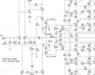
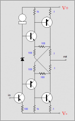
I am following this thread with great deal of interest. During the posts I saw some shematics for Technics new class A. Because some years ago I repaired on SE-A5MK2 I reverse engineer the sychro bias in the AMP responsible for new class A. I do not know if you have it or know it. Anyway I attach it (I believe it is correct.). Note that the vbe part is not the bias adjust circuit from se-a5. I added it as a conventional bias adjusting circuit. This is the think you are descussing, isn't it?. Sorry for interrapting anyway.
I am following this thread with great deal of interest. During the posts I saw some shematics for Technics new class A. Because some years ago I repaired on SE-A5MK2 I reverse engineer the sychro bias in the AMP responsible for new class A. I do not know if you have it or know it. Anyway I attach it (I believe it is correct.). Note that the vbe part is not the bias adjust circuit from se-a5. I added it as a conventional bias adjusting circuit. This is the think you are descussing, isn't it?. Sorry for interrapting anyway.
Attachments
Kzeprf22,
Prevoius posts have shown the concept of Tecnics A+ design, where you get a floating power supplied small class-A amp with a high power (4times more) AB amp output connected to the common supply terminal of class-A.
I think we can classify 3 major types:
1. Dynamic/sliding biasing scheme as shown in Nelson pass patent, LT1166, Pioneer patent etc. The bias ckt itself generates bias in sliding mode and also facilitates somewhat non-switching function of the power transistor. This goes in Vbe multipler position.
2. The other is: you keep your regular vbe multiplier or thermaltrak diode bias (rmi-fc100) and then add two diodes and resistor at the base of the power transistor connecting to ground. This allow you to retain your normaL class AB amp as it is but adds nearly non switching operation of AB amp during class-B operation. This has been shown by OS in his Frugal amp in previous post. This was found from technics IC SV2004 series reverse engineered chip internals.
3. technics class A+. Completely different topology. Also not an AB amp although it has got class B amp embedded in it.
The non linera bias generator menat to be thermally intolerant to during its operation while playing high input programme material. However, this is in theory. In practice this also suffers from Thermal Distrotion like any class-AB amp. In this regard ONsemi thermaltrak transistor based solution like rmi-fc100 can be worth looking at for further investigation.
The dynamic biasing is achieved , generally, with some non linear sub-ckts. This non linear bias controller are not able cope well with rail induced x-over distortions during high music picks, IMHO.i.e. low bias current defeats to the high programme material demand. In this regard Technics A+ is immune to rail induced distortion.
Later..
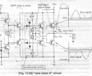
here is another one worthwhile to investigate. JRB has confirmed a 20dB less distortion in simulator. This is also non switching output.
http://www.tubecad.com/2006/12/blog0091.htm
http://www.tubecad.com/2006/12/blog0091.htm
Attachments
atiq19,
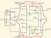
The design I attached is not reverse engineer from an IC is from a big discrete power amplifier, using sychro bias (new class A). The one you mention is also (new class a)? Witch one is the correct? In the Amp I am talking about the synchro bias was between the VAS and the drive transistors.
The design I attached is not reverse engineer from an IC is from a big discrete power amplifier, using sychro bias (new class A). The one you mention is also (new class a)? Witch one is the correct? In the Amp I am talking about the synchro bias was between the VAS and the drive transistors.
- Status
- Not open for further replies.
- Home
- Amplifiers
- Solid State
- The Frugalamp by OS