unlike mosfets the triple is cheaper for same linerity
In that image the d self triplet(3a)(douglas self) has biggest bandwith of all but I think is little tricky to make it stable.
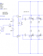
If we talk about that image like an matrix we can asociate 1 2 3 for columns and a,b for lines 😀
2a and 3b it gives least distortion.They are loading vas verry little unlike the others.You can simulate and study.I use now 2a (I'm satisfied about sound);it is stable because parasitic capacitor b-c is coupled at the ground from input.If you can do more you can put at most 10pf in parallel. but I want to go for 3b (not for superior sonic ,for easyast way of implementation of parallel output devices).But i think that is not so stable like 2a(just my theoretical say that ),practically I didn't try yet.
Instability comes because the driver of the final stage has big cb capacitance.If you look in the 2b from output to input we have the signal path from collector q90 then c2 then collector q97 and then c1 and base q97.In that case at higher frequency the output is turning in input in phase so you can make an oscillator 😀 That why the sziklai is litlle instability. But ...
But the problem can be resolved by chosing the corect q97 with litlle cob like 16pf -> 2pf (c5171 ,2sa1360 etc those used in video amplifiers etc).
The 2b version is still good thd<0.0004 .i prefer to use sziklai(cfp) in output because oftheir sound and advantages.
To obtain such linerity and gain(current in transient mode) with mosfet we have to buy lateral mosfets ,very expensive(10$ piece).that why I prefer bipolars .
ostripper:"Also any insight to how you T-comp the stages would be";I'm not understanding what you want,a picture ?
In that image the d self triplet(3a)(douglas self) has biggest bandwith of all but I think is little tricky to make it stable.
If we talk about that image like an matrix we can asociate 1 2 3 for columns and a,b for lines 😀
2a and 3b it gives least distortion.They are loading vas verry little unlike the others.You can simulate and study.I use now 2a (I'm satisfied about sound);it is stable because parasitic capacitor b-c is coupled at the ground from input.If you can do more you can put at most 10pf in parallel. but I want to go for 3b (not for superior sonic ,for easyast way of implementation of parallel output devices).But i think that is not so stable like 2a(just my theoretical say that ),practically I didn't try yet.
Instability comes because the driver of the final stage has big cb capacitance.If you look in the 2b from output to input we have the signal path from collector q90 then c2 then collector q97 and then c1 and base q97.In that case at higher frequency the output is turning in input in phase so you can make an oscillator 😀 That why the sziklai is litlle instability. But ...
But the problem can be resolved by chosing the corect q97 with litlle cob like 16pf -> 2pf (c5171 ,2sa1360 etc those used in video amplifiers etc).
The 2b version is still good thd<0.0004 .i prefer to use sziklai(cfp) in output because oftheir sound and advantages.
To obtain such linerity and gain(current in transient mode) with mosfet we have to buy lateral mosfets ,very expensive(10$ piece).that why I prefer bipolars .
ostripper:"Also any insight to how you T-comp the stages would be";I'm not understanding what you want,a picture ?
Attachments

MJL21193 said:
Important to remember that a sub operates at a very narrow band width and doesn't need to be ultra fast or ultra low distortion, it NEEDS to be stable and durable. Rod's "primitive" circuit is just that. Anything more is a wasted effort.
I'm totaly agree or more than that 🙂 .
By MJL - Rod's "primitive" circuit is just that. Anything more is a wasted effort.
The p68 works good ... , if you don't know how to do any better.
But we DO know better... Rod even says it is for "light intermittant" duty. I do not use my stuff either light or
intermittant. No VBE ,no cap on the CCS, a bootstrapped 15033 VAS, c'mon. 3-4$ more parts (stimulate the economy) and
good things happen.
Who knows you might replace your sub with a full range
but have to scrap your "sub" amp for the sake of a
little "wasted effort".
By MJL - sub operates at a very narrow band width and doesn't need to be ultra fast or ultra low distortion
Ultra low distortion , I agree.. but fast (slew), it should be . Also
a sealed 12" peerless dips to 2R , so a killer OPS should
be used (triple or mosfet). Durable... that APT /wilson input/VAS is
totally IDIOT proof (lamer proof too 🙂 ) but can do -120db
H2 with most OPS's.. A whole 5 .10c'ers and 4 .40c trannies
won't break the bank either. I Shorted a output on one of them
and spilled a beer on the other... they still live
 .
.Also for THIS sub , offset protection and MJL quality PCB's are a MUST..
OS
By catalin - 2a and 3b it gives least distortion
I really like the idea of "3b" (the last one).
would device paralleling be good on it???
is stable because parasitic capacitor b-c is coupled at the ground from input
that one you will have to draw out ( it seems to be coupled to the rails/op C??) ground ....dirty ground.. or signal ground??
would you use the parasitics on the negetive side as well
(symmetrical)?
OS
Hi OS,
Just a note - beware of bad power MOSFET models! The original SPICE MOSFET models (NMOS levels 1, 2 and 3) are for the type of MOSFET found in ICs - the lateral type. But the IRF devices are the vertical type. For lateral MOSFETs, Cgd (same as Crss) is almost constant with Vgd, while Cgs varies quite a bit with Vgs. For verticals, Cgd (Crss) varies quite a bit with Vgd and Cgs is almost constant with Vgs. This variation of Cgd with Vgd for verticals can cause problems in the real circuit that the simulation will not show if the standard NMOS models are used. Briefly, the input capacitance of the output stage is minimum near 0 Volts out, and increases quite a bit as the output approaches either rail. So the output stage bandwidth (and therefore overall stability of the amp) decreases as the output approaches the rail. For more info, see the LTspice documentation for the VDMOS model (an LT-specific model that addresses the capacitance issue).
Also, the driver arrangement should be the same as what you'd use for a BJT output stage - a single resistor between the driver emitters (no connection to the output) in parallel with a capacitor. The capacitor will speed up turn-off of the output stage and help prevent common-mode conduction just like it does with BJTs.
In addition, the IRF P-channel devices have a strange behavior. Their transconductance varies a lot with frequency even in the audio band. No SPICE model will predict this, and it's undesirable. But on the bright side, only IRF P-channel devices have this problem. Fairchild P-channel devices don't have the problem, and as an added bonus, they're cheaper than the IRF P-channel devices at Mouser.
By andy c. - only IRF P-channel devices have this problem. Fairchild P-channel devices don't have the problem, and as an added bonus, they're cheaper than the IRF P-channel devices at Mouser.
Are the fairchild models for MOSFET's any better ,I haven't ordered yet.. any recommendations for p/n
15A+ devices??
Also, the driver arrangement should be the same as what you'd use for a BJT output stage - a single resistor between the driver emitters (no connection to the output) in parallel with a capacitor. The capacitor will speed up turn-off of the output stage and help prevent common-mode conduction just like it does with BJTs.
That is a new one.. makes sense , but the quasi amps reference
from op, haflers and most others don't.. majority wins..
how you would implement gate protection without a reference
is the only issue now😕 😕
ostripper said:
I really like the idea of "3b" (the last one).
would device paralleling be good on it???
that one you will have to draw out ( it seems to be coupled to the rails/op C??) ground ....dirty ground.. or signal ground??
would you use the parasitics on the negetive side as well
(symmetrical)?
OS
Yes ,paralleling is good on it 3b .practically i didn't tested,i just waiting for time.3b get more current in input(but little diferencies) for the same current output unlike 2a.
The 2a is coupled to rails but i don't want to draw out(all ef do that 😀).The sound is super at 2a and is stable.Even 2a could be paralleled with 4.7 ohms from emitter second stage to all the collectors of the parallel transistors .
ostripper said:Are the fairchild models for MOSFET's any better ,I haven't ordered yet.. any recommendations for p/n
15A+ devices??
I don't think the Fairchild models are any better. Recommended part number for the P-channel device would be FQA12P20. I have some models for the IRFP244 and FQA9P25 (which are similar to the IRFP240 and FQA12P20), that model the varying capacitances pretty well.
That is a new one.. makes sense , but the quasi amps reference from op, haflers and most others don't.. majority wins..
I'm not sure what the "quasi amps reference from op" is, but if it's a quasi-comp design, that's a somewhat different beast from a complementary design. I'm sure it would have some considerations specific to that type of topology. I haven't looked into quasi-comp designs to be honest.
how you would implement gate protection without a reference is the only issue now😕 😕
Have a look at the manuals at hafler.com. For example, the DH-500 manual is here (PDF). You'll see the protection diodes are connected from the driver bases to the output. This is a better design anyway, because if these diodes are connected to the driver emitters, there's nothing to limit their current when they turn ON. When connected to the driver bases, the max output current of the VAS limits the max current in the diodes. There's no capacitor between driver emitters in that design though.
If you wish to evaluate the effect of the capacitor on common-mode conduction, you can use a simulation similar to that below. Not all devices are shown, and the load is not shown, but should be present. Run the output amplitude somewhat below clipping, and the frequency to 100 kHz or more. Look at the drain currents of one each N-channel and P-channel devices on the same plot. Change the sign of any drain currents as necessary so that they are both positive in polarity on the graph. At low frequencies, the drain currents will intersect at exactly the bias current, as expected. But as you crank up the frequency, the intersection point will reach a higher and higher current, because of the "other" device not turning off soon enough. This is an objective way to look at it without having to resort to "majority rule" - but you need good models. Check out how the driver bias current, driver capacitor value and MOSFET gate resistors affect this.
Please excuse the polarity of the Vgs voltage sources in the diagram. The Vbias voltage parameter is negative for each one. I oriented them this way so that the currents through the voltage sources had the polarity I wanted without having to put minus signs in there when plotting them.
Attachments
ostripper said:
The p68 works good ... , if you don't know how to do any better.
But we DO know better...
We like to act like we do...🙂
ostripper said:
Rod even says it is for "light intermittant" duty. I do not use my stuff either light or
intermittant. No VBE ,no cap on the CCS, a bootstrapped 15033 VAS, c'mon. 3-4$ more parts (stimulate the economy) and
good things happen.
Who knows you might replace your sub with a full range
but have to scrap your "sub" amp for the sake of a
little "wasted effort".
Rod says that a sub amp that is not handling the full audio spectrum will be seeing intermittent duty. This is for heatsink size and cooling not performance. Run an amp for full audio spectrum and compare the heat dissipated to one that is only doing high power sub work - the sub amp runs substantially cooler.
Looking at the design (again) the amp is running class B so no, there isn't a vbe multiplier, just a diode string. A cap on the CCS? Why?
Once again, a high power sub amp doesn't need the bells and whistles that a fullrange amp should (to mostly make one feel better about it) have. Bootstrapping takes a back seat to nothing and using a big ol' MJE15035 as VAS is neither here nor there for this type of amp as you will not differentiate an improvement audibly. Anyway, his 3A uses (optionally) an MJE15035 for VAS and it's fairly well regarded.
It's not about economy so much as availability of parts, stability (paramount in a big amp) and ease of construction. Couple this with the very real idea that the amp doesn't need to be better than it is for the range it will operate in.
ostripper said:
Ultra low distortion , I agree.. but fast (slew), it should be . Also
a sealed 12" peerless dips to 2R , so a killer OPS should
be used (triple or mosfet).
Say a maximum of 150Hz, why would it need to be fast?
Fast enough it is anyway - MJE15035 ft=30MHz, outputs are fast too.
Impedance dips are handled by the max dissipation of the output stage. Mine handled an impedance dip of 0 ohms when I accidentally shorted the output to ground and melted (solid wire) board traces and tripped the 15 amp breaker at the main panel. Didn't lose any outputs though (MJL21193/94 inspired my forum name with their toughness).
andy_c said:In addition, the IRF P-channel devices have a strange behavior. Their transconductance varies a lot with frequency even in the audio band. No SPICE model will predict this, and it's undesirable.
Andy,
Nelson Pass uses these in his amps to glowing reviews & I have a Greg Ball SKA amp with IRFPs in O/P stage which sounds excellent. I'm sure there are many other fine sounding amps using these devices. How does this square with what you say?
Can you provide any test results to verify your statement? Just as a means to delve into this anomaly that you have identified.
jkeny said:
Andy,
Nelson Pass uses these in his amps to glowing reviews & I have a Greg Ball SKA amp with IRFPs in O/P stage which sounds excellent. I'm sure there are many other fine sounding amps using these devices. How does this square with what you say?
Can you provide any test results to verify your statement? Just as a means to delve into this anomaly that you have identified.
The negative feedback in amps makes up for any variation in transconductance.
I have numerous home build amps with these devices in and they all sound very good.
OK, I understand that but I thought N Pass amp building philosophy was to get the least distortion build before applying feedback. If only the IRFP devices show this transconductance variation, then why choose them from among the many other mosfets that avoid this issue? Is there some other compelling advantage for them?
jkeny said:Andy,
Nelson Pass uses these in his amps to glowing reviews & I have a Greg Ball SKA amp with IRFPs in O/P stage which sounds excellent. I'm sure there are many other fine sounding amps using these devices. How does this square with what you say?
Can you provide any test results to verify your statement? Just as a means to delve into this anomaly that you have identified.
Oh, I didn't identify this at all. It was Nelson who did. It is shown in figure 13 of this article.
I referred to this behavior as "undesirable", and did not say it was impossible to make a good amp with them. The behavior of the IRF P-channel devices has been discussed many times in this forum over the years. The N-channel devices don't do this.
Ok Andy, thanks I hadn't heard or noticed this before - I'll have a read. There must be some compelling reason to choose these devices so?
jkeny said:Ok Andy, thanks I hadn't heard or noticed this before - I'll have a read. There must be some compelling reason to choose these devices so?
I use them coz they are high current and high voltage devices.
- Status
- Not open for further replies.
- Home
- Amplifiers
- Solid State
- The Frugalamp by OS