bullittstang: Will do this tomorrow morning. Have checked the PSU outage to the amp splitter without boards attached and it is very even and steady at right around +/- 25.8 vdc. Only when the boards are connected does the phenomenon noted above occur.
Probably best to head right for the hardware store in the morning to collect parts for DBT.
OK, good morning, DIYers. Will offer two posts, one with the requested PSU info and the second with grounding info.
First, the PSU was disconnected from the amp and the AC Transformer Out and Rectifier DC Out were measured. Both are a little high:
Top Wind: Transformer AC=19.37V; Rectifier Out=25.81VDC
Bottom Wind: Transformer AC-19.34V; Rectifier Out=25.86VDC
Then the cable was connected to the Amp chassis, the two boards were disconnected from Gnd, Vpos and Vneg, and the voltage checked: +25.80VDC and -25.79VDC. Have reported these figures before. These VDC values were stable and did not fall.
Then, the Right, working channel was connected and the Vpos and Vneg values checked. They both started out around +/-25.4, then, after a few seconds began to fall in tandem (both + and -).
This is happening with both boards and indicates some problem, perhaps a ground one as suggested by the helpful bullittstang.
So, next post, what I know about the grounding.
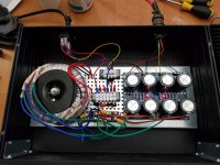
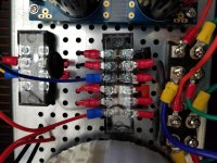
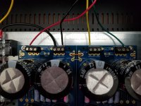
And here are photos of the PSU unit that has never been a problem (so far, at least).
First, the PSU was disconnected from the amp and the AC Transformer Out and Rectifier DC Out were measured. Both are a little high:
Top Wind: Transformer AC=19.37V; Rectifier Out=25.81VDC
Bottom Wind: Transformer AC-19.34V; Rectifier Out=25.86VDC
Then the cable was connected to the Amp chassis, the two boards were disconnected from Gnd, Vpos and Vneg, and the voltage checked: +25.80VDC and -25.79VDC. Have reported these figures before. These VDC values were stable and did not fall.
Then, the Right, working channel was connected and the Vpos and Vneg values checked. They both started out around +/-25.4, then, after a few seconds began to fall in tandem (both + and -).
This is happening with both boards and indicates some problem, perhaps a ground one as suggested by the helpful bullittstang.
So, next post, what I know about the grounding.
And here are photos of the PSU unit that has never been a problem (so far, at least).
Attachments
Here's what I have fathomed about the grounds so far. The PSU PCB shares the ground from the power in to the board – that ties both the Vpos and Vneg grounds together (as recommended). The ground is then transferred to the amp chassis and fed to the Gnd.P on each board. This creates a common ground throughout the entire amp chassis and the checks done so far show a common ground between the mosfet screws to the heatsink, to the back panel ground speaker and RCA connectors, and to a few other checkpoints. Don't know what to check, specifically, and am trying the obvious.
The PSU chassis is not grounded – the active ground is from the PCB to the Power Switch Gnd and the Transformer and Rectifiers are isolated from the metal frame (carefully so). So the chassis of the PSU does not share any Gnd with the Amp chassis. The Amp chassis has an active Gnd created, somehow, by the Boards and, I presume, by their connection to the heatsink.
The voltage is dropping when (and only when) the boards are connected with no load. If this is a problem, then let me know, otherwise, I assume that it is normal.
Thanks, all. This has been a long process and is taxing my abilities. Your help is, therefore, very much appreciated.
Got the parts and will build the DBT today. In the meanwhile, noted that the RCA jacks had been installed, perhaps, incorrectly so that their ground metal plate touched the metal backplate. Rearranged this so it agreed with the ACA build and the RCA ground was distinct from the chassis ground -- which it now is. Restarted the amp with power and it had the same smoke appearing at 1:45. Wonder if the ground problem could have blown the mosfet on the left channel side.
This is a bear. Am also thinking that none of the board voltage checks can be made without a speaker load. Is this correct? Don't have a 4 or 8 ohm resistor available and also wonder if it should be 3 watt when used as a speaker load substitute.
This is a bear. Am also thinking that none of the board voltage checks can be made without a speaker load. Is this correct? Don't have a 4 or 8 ohm resistor available and also wonder if it should be 3 watt when used as a speaker load substitute.
Last edited:
You do not need any load, that will only make the voltages “off” or the smoke appear quicker.
You did set the bias and check that on the board right? This sounds like it is being overdriven, which would take a minute or two to come up to full bias and start overheating parts without any load attached.
Asking so we don’t skip the basics, since it sounds like the supply voltages are good.
You did set the bias and check that on the board right? This sounds like it is being overdriven, which would take a minute or two to come up to full bias and start overheating parts without any load attached.
Asking so we don’t skip the basics, since it sounds like the supply voltages are good.
A speaker load is not necessary for making DC voltage checks. It is a Class A amplifier, so the speaker is nothing more than a temporary diversion of current away from the OS transistors.
Start back with the fundamentals:
On the working channel board (and only the working board), confirm the DC offset across the speaker terminals is sufficiently small (< 50mV, or better ~ 10mV), with no load. Then check the DC bias current by measuring voltage across the power resistors on the PSU board. The bias current is set by the opto-isolator circuit and should be close to 1.3 Amps. There is no adjustment for the bias current.
Now power down, let the PSU cool off. Then connect the problem board, and only the problem board. Repeat the above measurements, quickly. Power down as necessary to avoid smoke. Ideally the bias current measurement should be made from a cold start, watching as the channel board powers up. The opto-isolator takes several seconds to stabilize due to the big cap. The idea here is to make note of any differences in the fundamental circuit parameters, output offset and DC bias current, between the two channel boards.
Build the DBT and put in a 60-100w bulb and you should be able to run for much longer without smoke.
Keep in mind the DBT will decrease voltage the higher the current going through it, so any prior voltages may be a little higher or a lot higher than voltages you get with the DBT attached.
Keep in mind the DBT will decrease voltage the higher the current going through it, so any prior voltages may be a little higher or a lot higher than voltages you get with the DBT attached.
TA: On both boards, the voltage is dropping over time. Will that affect the dc offset and power resistor measurements? Checked the DCV on the good channel and it is too low -- roughly -210mv. This is with the MountainView card inserted. Should the 2 to 4 short be used instead? Am starting to get lost with all of the problems.
One board only. Do the measurements. Disconnect first board, connect second board do the measurements. trust the procedure. And relax it is only a circuit.
Yes, to Signal lost you listen. 😉
The FE card does not affect the DC parameters of the output stage. It is isolated by two AC coupling (aka DC blocking) capacitors. So Mtn View is same as Ishikawa is same as Tucson, etc. The DC offset and final bias current will take a while to settle down. At least 10 minutes. Leave it on for another 20 minutes. Check again. Leave for an additional 30 minutes (or one hour total). Then perform the final confirmation.
The FE card does not affect the DC parameters of the output stage. It is isolated by two AC coupling (aka DC blocking) capacitors. So Mtn View is same as Ishikawa is same as Tucson, etc. The DC offset and final bias current will take a while to settle down. At least 10 minutes. Leave it on for another 20 minutes. Check again. Leave for an additional 30 minutes (or one hour total). Then perform the final confirmation.
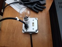
OK, got the DBT done and it was not difficult -- but many of us have noted that Home Depot prices have gone through the roof. See photo.
Connected the PSU to the DBT and turned it on -- the first time, the light shone briefly then went dark.
Then tried the amp with the good channel only active. No dim bulb and, I guess, that means no short, right?
Then tried just the trouble channel and it too did not light up the bulb.
So I am guessing that we are not dealing with a short, here. Is this right?
TA: Am feeling overly frustrated because everything I have tried for the last 3 weeks has failed on this amp. Am going to take the rest of the day off and try to recover. Tomorrow I will see if it is possible to get the right channel DC offset down and then measure the power resistor. Is this R13 or R14?
Thanks, DIYers.
Attachments
The power resistors are the ones shown in the schematic between the mosfets and the speaker output.
Please don't think I am picking on you. To me it seems like your trouble shooting technique is very erratic and lacks a pattern that would help you figure out the problem. Assume that nothing is working correctly. Measure the non smoking side against the smoke producing side. Somewhere in those measurements is the clue to the problem. Hang in there and you will figure this out.
Please don't think I am picking on you. To me it seems like your trouble shooting technique is very erratic and lacks a pattern that would help you figure out the problem. Assume that nothing is working correctly. Measure the non smoking side against the smoke producing side. Somewhere in those measurements is the clue to the problem. Hang in there and you will figure this out.
^ Again, excellent advice.
Also a good idea to take a step back when the frustration level becomes excessive.
Another place to measure the bias current is across the four power resistors on the PS board. With a single channel board under test, this current should equal (very nearly) the current across the power resistors in the output stage.
Too many cooks spoil the broth but if troubles continue and high current is still roasting resistors, I have some suggestions.
As Tungsen Audio mentioned, the DC current is set by the optocoupler bias control circuit.
The bias control previously did not seem to be working as it has been mentioned that R11 and R12 had smoked, as had R13 and R14.
Since R11 and R12 smoked, it suggests to me that the optocoupler 4N35 may be faulty. It may be bad solder joints or damage from overheating or possibly static. I suggest replacing it. Also consider installing a socket on the board for the optocoupler to eliminate the possibility of damaging the optocoupler by overheating. The only other active components are the two voltage references Q6 and Q7 (LM385) that may be damaged, so replace those too. Also check that C3 is oriented correctly for polarity.
Additional voltage check would be to connect meters to the Gate and Source pins of the Mosfets to measure the Vgs applied to the Mosfets. At power-up, they should read zero Volts, and then rise as the optocoupler circuit activates. When fully active it should be at approximately 4.4 or 4.5V. It may be less with the DBT in place. If significant voltages are measured at Gate/Source at power-up or if the measured voltage is much higher than 4.5V after a short period of time, then there is something wrong with the optocoupler bias circuit.
I was also starting to suspect a faulty optocoupler bias circuit in the problem board. And possibly a blown or otherwise shorted 3300 uF capacitor. But this is jumping ahead of proper diagnostic investigation.
No problem. 🙂
Craigl59 has been having issues for about two weeks now so I thought I would mention a possible cause.
Craigl59 has been having issues for about two weeks now so I thought I would mention a possible cause.
BenMah: Thanks for the info. Am learning as I stumble through and your comments are helpful. R11 and R12 were, BTW, blown because the original build reversed the mosfet positions. The optocouper was replaced twice on this board and the second, new board has another one on it.
Signal lost: your troubleshooting advice is helpful AND it is important to stress that my technique is not "erratic" but, rather, that I have NO technique at all. That is why the specific suggestions offered are helpful. Can learn, try them out, and report the results. Assuming that everything could be wrong is wise advice and my issue is that I do not know what everything is -- this is the first time I have attempted a build this complicated and had I known that developed technical skills were required, would not have taken the plunge.
TA: Replaced both the Optocupler and the 3300 capacitor on the last redo of the initial card and it still started smoking on the other end -- around RV1. Your help is most appreciated and well presented.
Some board data, finally.
Got the (working) right channel adjusted to -0.044dc offset. Removed the RCA short and then measured R14 -- it rose to 602mv and stabilized. Measured R13 and it was exactly the same: 602mv.
Then got the (faulty) left channel dc offset adjusted as best as possible -- cannot leave it on long enough to stabilize but it was between -0.040 and +0.030. Removed the RCA short.
Measured R14 first and it just kept getting higher -- stopped at 1.2VDC to make sure no smoking occurred.
Let it cool off then measured R13 -- same result and also stopped at 1.2VDC. But they were headed towards smoking, could tell.
So, what causes this out-of-control rise? Is it the Mosfets? They are new on this new board and carefully soldered. Can it be the Optocoupler? It is also new and care was taken to line up pin 1.
The bright minds on this forum will know and, perhaps, tell me.
Last edited:
- Home
- Amplifiers
- Pass Labs
- The diyAudio First Watt M2x