Just to be, perhaps, helpful, here are the changes made to the build parts for the second, new left board -- that is smoking.
1. the recommended 10uf green non-polar cap C2 was unavailable so selected a Nichicon Aluminum Electrolytic 10uf, 50V, at 20%.
2. CB3 has not been available for any of the 4 cards built so far and, so, substituted a WIMA film capacitor, 1.0uf 50VDC, 5%.
3. The RV1 5k trimpot has also been back-ordered everywhere and, so, substituted a Bourns 5k through hole trimmer resistor -- also W type, 3pin inline. Works on the other board but will be switching to the 20k trimmer + 137k resistor change to solve the minus dc offset problem.
Let me know if any of these substitutions might be causing problems.
Substitution of a polar electrolytic for a non-polar electrolytic could be a big problem. Which way did you orient the PC? You may find this page instructive.
What Happens if We Connect a Polar Capacitor the Wrong Way?
What Happens if We Connect a Polar Capacitor the Wrong Way?
That can be a way to find out what the scoring lines in the top of electrolytic caps are for. Even if they don’t vent their insides, polar capacitors that are reverse biased get hot as a result of conducting DC current.
Some board data, finally.
…
Then got the (faulty) left channel dc offset adjusted as best as possible -- cannot leave it on long enough to stabilize but it was between -0.040 and +0.030. Removed the RCA short.
Measured R14 first and it just kept getting higher -- stopped at 1.2VDC to make sure no smoking occurred.
Let it cool off then measured R13 -- same result and also stopped at 1.2VDC. But they were headed towards smoking, could tell.
So, what causes this out-of-control rise? Is it the Mosfets? They are new on this new board and carefully soldered. Can it be the Optocoupler? It is also new and care was taken to line up pin 1.
Well, that left channel is hosed for sure. The optocoupler bias circuit is not functioning correctly. The Mosfets may still be Ok. The polar cap used in the place that calls for a non-polar is probably not Ok.
Craig
I just measured the voltage drop on the R14 for other reasons and I find 630mV. So it seems your amp is drawing twice as much as mine.
I just measured the voltage drop on the R14 for other reasons and I find 630mV. So it seems your amp is drawing twice as much as mine.
Yup. The right channel looks Ok, but the left channel is drawing twice what it is supposed to. There are a number of protection devices around the optocoupler bias circuit that are supposed to prevent this. The diodes and voltage sources need to be checked in addition to the optocoupler itself.
TA: Mentioned the 10uf, 50V substitution some time ago and got no response -- assumed it was OK and the long leg was placed in the + side as indicated on the cap position (close to the transformer). The UES1H100MPM BoM cap is unavailable at both Mouser and Digikey and think that if it is required for proper board construction, then noone will be building M2xs for a while.
If the board is hosed, it has happened with no problems that I am aware of. The voltage across R13 and R14 is not at 1.2VDC, that is just where I stopped measuring. It continues to go up. Will check the diodes. What are the voltage sources?
If the board is hosed, it has happened with no problems that I am aware of. The voltage across R13 and R14 is not at 1.2VDC, that is just where I stopped measuring. It continues to go up. Will check the diodes. What are the voltage sources?
Just checked the diodes and they are fine. If there are any other possible causes for this continual rise in DCV around R13 and R14, please let me know.
Again, the 2nd, new board was prepared very carefully and can be seen in post 5415 above. Cannot fathom why it is hosed if there is no problem with the board -- unless the optocoupler sent by Mouser is defective. Don't know how to check this.
Again, the 2nd, new board was prepared very carefully and can be seen in post 5415 above. Cannot fathom why it is hosed if there is no problem with the board -- unless the optocoupler sent by Mouser is defective. Don't know how to check this.
"will be switching to the 20k trimmer + 137k resistor change to solve the minus dc offset problem"
I do not know if this is a mistake in post or you actually installed 137k. It should be around 37k
I do not know if this is a mistake in post or you actually installed 137k. It should be around 37k
Yes, 37k is correct and are the resistors I have from Mouser. Thanks for the clarification. This correction has not yet been applied. Am trying to find out the problem with the new board and what is causing the continual DCV rise around R13 and R14. In the build of this board all of the resistor values got checked carefully and once again after installation.
Last edited:
See here and some posts below
My browsers (Chrome, Firefox) can't display the image embedded in post #3867.
In case it happened to be a schematic of the M2x amplifier channel board, I've attached another of those below.
_
Your board is still salvageable, but definitely not functioning correctly. The voltage references are parts Q6 and Q7. They are for 1.2V
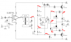
Here is the schematic (containing test point names) that darr was referring to. Mark J. gives some good tips on how the M2x operates, and how to make some additional measurements in this post: The diyAudio First Watt M2x
The cap you used at C2 slipped under the radar because of the notation on the schematic. You will still want to replace with a recommended bi-polar "green sleeve" style component. That means a Nichicon UES series bipolar. There are a few replacements that will work. In 10 uF you can use a 35V or 63V part if 50V is unavailable. It is also possible to use a 22 uF part in 35V or 50V.
Attachments
Craigl59:
Here are two more measurements you can take to come closer to solving the bias circuit / optocoupler mystery:
with the amp OFF,
- please measure the resistance between R13 and optocoupler Pin1. It should be something in the vicinity of 100 Ohms.
- please measure the resistance between R14 and optocoupler Pin2. It should be something in the vicinity of 320 Ohms.
What do these measurements tell us ?
First, some conceptual explanation;
The LED in the optocoupler (between pins 1 and 2) givesa signal about the actual current to the transistor in the optocoupler, which then opens more or less (has more or less resistance). This allows the big 3300uF capacitor, that is parallel to the transistor, to reach a certain voltage.
More current through the Q1 / Q2 MosFets, LED in the optocoupler shines more brightly, phototransistor in the optocoupler opens more (less resistance) and hence pulls down the voltage of the 3300uF capacitor, closing MosFets Q1 / Q2 down somewhat. This way, a regulation loop is established that aims to keep the MosFets at about 1.3 amps of current. The loop has long time constant, that is why you see on your good board current rising to 1.3 amps slowly ( about 600mV over R13 / R14), and then stabilizing there when the loop is in its steady state.
Here, the resistances I suggested to measure would give you some information if the circuit thorugh the optocoupler LED is correct, and can make the LED illuminate with brightness according to the current through R13 and R14. The circuit would R13 - R10 - Opto LED - R11 - R12 - R14. If this circuit is not closed or the resistances are wrong, the Opto LED can never illuminate properly to tell the phototransistor to regulate the current through Q1 and Q2 down, and it would keep rising.
So, I'm interested in your resistance measurements as suggested above.
Hope this helps,
best regards, Claas
Claas: Superb post; cannot thank you enough.
Checked R from R13 to pin one and it is 100.4. Then checked from R14 to the pin below 1 (assume this this is 2) and it is 220.7 -- too low, right? The R from R13 to pin 2 is, also, 220 (don't know if this is relevant).
Does this suggest the nature of the problem? Understand your clear explanation of the regulation loop and this type of explanation is very helpful to those of us just starting to understand the circuit.
Thanks again, Claas.

Check the resistors Claas notated in order and provide their resistance, looks like one of them is bad
OPTO-R11-R12-R14, one of those from R11-R14 might be out of spec.
OPTO-R11-R12-R14, one of those from R11-R14 might be out of spec.
TA: Thanks as well for your "always superb" posts. This is the current cap:
https://www.mouser.com/ProductDetai...GzmEl62sI15kdP1fQBjspIa9ytddIFUZXhi3OhJGKew==
It is a bi-polar/non polar electrolytic cap. So should it still be replaced?
Will download and study the schematic with additional info.
Please see Claas's post and my response above and tell me if this suggests a path forward.
Checked R10=100.9; R11=220.7, and R12=100.9. All correct. All resistors were checked when installed and were within spec. R13 and 14 are, of course, 0R47.
What else could contribute to the low R between R14 and Pin2?
What else could contribute to the low R between R14 and Pin2?
Last edited:
OK, checked the R from R14 to Pin 2 on the working, right channel and it is 322 -- within Claas's spec. Then checked another new board, the right channel built at the same time as the left trouble board, and it reads 220 -- the same low R as above. Does this suggest that the 78-4N35 optocouplers Mouser sent me in the last batch are defective? Can there be any other build issues that would cause this low R?
Thanks, folks. We are making progress.
Thanks, folks. We are making progress.
Hmm ... could be that Q6, Q7 or the Opto LED are messing with the resistance measurement.
Could you redo the R14 to Opto Pin2 measurement with multimeter leads reversed ? Actually, try the leads in both directions - red on R14, black on Pin2, and the other way around. Is there a difference ?
While the too-low resistance you measured for R14 - R12 - R11- Pin2 certainly is an interesting data point, it would move the regulating action of the optocoupler bias circuit in the opposite direction: lower resistance in these paths would provide the Opto LED with more current for a give voltage over R13 / R14, and hence provide stronger illumination of the photo transistor, leading to it becoming more open already at a lower voltage through R13 / R14 -> bias is regulated to a lower resulting current.
So that is not your main culprit, unfortunately ...
The measurements across the resistor do show us that the Opto LED should get voltage / current once there is current flow through Q1 and Q2.
That the current measured over R13 / R14 is riding slowly suggests that the 3300uF capacitor C3 is functioning also as it should.
That leaves as the culprit for the mis-functioning bias cicuit :
1) the optocoupler itself.
- is it really inserted correctly ? could you post some well-lit, high resolution photo of the optocoupler area where we could see its orientation ?
- optocoupler is defective - soldered too hot ? gotten too high of a voltage in one of the starts where the current got so high that R13 / R14 started to smoke ?
- optocoupler wrong part - it is a 4N35 ?
2) the phototransistor side of the optocoupler does not provide a parallel path to the capacitor C3, limiting the voltage to that it gets charged by diverting current through the opto transistor.
- is there continuity (low resistance) between Opto Pin5 and C3 + ?
- is there continuity between Opto Pin4 and C3 - ?
- opto transistor defective ?
Also, another tip: When I am troubleshooting, I always have the schematic in front of me, and try to make sensefrom the paths and connections on the schematic and the points I measure.
Regards, Claas
- Home
- Amplifiers
- Pass Labs
- The diyAudio First Watt M2x