great results.
what output transistors did you finally use? have you considered the IPD320N20 of infineon ? (22nC, 32mohm,34A,200V)
what output transistors did you finally use? have you considered the IPD320N20 of infineon ? (22nC, 32mohm,34A,200V)
Some insights regarding the switching stage.
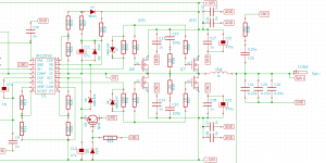
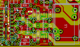
Please refer to the attached schematic and PCB.
The MosFets are two IRFI4212H.
Their specific beauty is the package, which allows low parasitic inductances, combined with an easy to handle fully isolated TO220-5.
It allows to keep small the critical half bridge loops:
Q6, C17, C18 and in the same way Q7, C13, C14
This keeps the intrinsic ringing frequency and damping high.
==> You get perfect signal integrity free of ringing already with very light snubbering.
Low Qrr of the IRFI types also keeps the situation nice during heavy load with hard switching conditions.
Downside of course is the very restricted portfolio of MosFets in this package.
Gate drive:
The shown values are the softest, but still reliable gate drive which at the same time allows to skip D7 & D8 for high end spectrum shaping.
Particularly in the mid power range (i.e. 10W into 4R) with D7 & D8 you will get some more high order harmonics, vs the posted spectrums.
However D7 and D8 are strongly advisable for heavy duty party operation into 2R, because D7 and D8 substantially reduce the switching losses at heavy loads.
During idle operation the losses are identical for both variations, no shoot through, no forced transitions, but nice ZVS.
Overall the idle losses of the main board are 3W, whereof 2W happen in the auxiliary supplies and small signal area.
Approx. 1W idle losses sum up in the MosFets and inductor.
Attachments
Very nice design. Do you have any idea what causes the extra harmonics with the extra diodes? Is it the extra asymmetry of switching timing (faster off with diodes)? If so, can it be tweaked with a different dead time setting?
Another question, not for implementing in this design, but have you ever tried a separate npn-pnp push-pull for gate driving? Especially if you parallel FET's this is very beneficial in my experience (in power electronics, remember, not class D designs).
Cheers, Marc
Another question, not for implementing in this design, but have you ever tried a separate npn-pnp push-pull for gate driving? Especially if you parallel FET's this is very beneficial in my experience (in power electronics, remember, not class D designs).
Cheers, Marc
It is a combination of dead time distortion and dv/dt shaping.... any idea what causes the extra harmonics with the extra diodes?
IMHO the dominant portion is the dead time.
Dead time has to defined more detailed.
There is the dead time of the driver IC and there is the time during which upper and lower MosFet are both non conductive, which I call effective dead time.
In order to avoid heavy brute force during removing of Qrr and avoiding exzessive dv/dt afterwards it is helpful to chose moderate high drive impedances for turning ON. In order to achieve low losses during turn OFF and (ensuring that the reverse transfer capacitance cannot cause unintended turn ON effects) it is often helpful or even necessary to turn OFF with lower impedances. In many cases this leads to effective dead times, which are longer than the dead time of the driver IC. Unpleasantly the effective dead time is also depending on the load.
A multiparameter optimization which becomes even more difficult with the restrictions in dead time setting the IRS....
Besides dead time setting of the IRS also the level of gate driver supply can be used to tune a little bit.
I would not dare to state that the shown solution is the ultimate, but it is one of the good performing options, so in the moment I tend to stay with it.
Yes, that's fine in class D as well.... ever tried a separate npn-pnp push-pull for gate driving? Especially if you parallel FET's this is very beneficial in my experience (in power electronics, remember, not class D designs).
In first step already the PNP can be of great help and for real heavy loads NPN and PNP.
Just have a look to the 2kW thread...
Thanks for the effort of elaborating. Very interesting. Every single detail you mention is relevant in power electronics too. I remember a design where I added an extra boost switcher in order to be able to meet minimum VCC for a gate driver IC and at the same time keep the rail for gate driving at a lower voltage. And then it all changes again when you start using SIC FET's. An interesting hobby/profession, isn't it 🙂
One thing that you might easily try: I'm used to very different gate on and off ratio's.
You could try 2E2 off and 2E2+22E on. That's usually a good starting point in my experience. I'm also used to snubbering with a much lower resistive part (sub 10E).
One thing that you might easily try: I'm used to very different gate on and off ratio's.
You could try 2E2 off and 2E2+22E on. That's usually a good starting point in my experience. I'm also used to snubbering with a much lower resistive part (sub 10E).
Last edited:
Some insights regarding the switching stage.
The MosFets are two IRFI4212H.
Their specific beauty is the package, which allows low parasitic inductances, combined with an easy to handle fully isolated TO220-5.
Choco
Have you looked at these ?
http://www.irf.com/product-info/datasheets/data/irfi4019h-117p.pdf
Won an cheap Chinese class-d last night off ebay and its fitted with one of those, to lazy to check do parasitic at the moment looks interesting as both fets are bonded into one package.
1pc IRS2092 Class D Mono 200W Amp Board | eBay
Every single detail you mention is relevant in power electronics too. I remember a design where I added an extra boost switcher in order to be able to meet minimum VCC for a gate driver IC and at the same time keep the rail for gate driving at a lower voltage. And then it all changes again when you start using SIC FET's. An interesting hobby/profession, isn't it 🙂
One thing that you might easily try: I'm used to very different gate on and off ratio's.
You could try 2E2 off and 2E2+22E on. That's usually a good starting point in my experience. I'm also used to snubbering with a much lower resistive part (sub 10E).
...I see - you are sort of addicted as I am.. 😀
Power electronics: ClassD amps are power electronics.
More precise in SMPS terminology most classD amps would be called high speed adjustable precision synchronous rectifying four quadrant buck converters.
2E2 off and 2E2+22E on:
Fine in terms of power electronics, but for low distortion this would need a driver IC which enables negative dead time at its output in order to achieve a very small effective dead time at the MosFets.
And if the driver would provide this - I would clearly prefer your proposal over the slowish turn OFF, which I am using here.
If you do it with the restricted options of the IRS your proposal will work reliably, but dead time distortion in the mid power range would be of average level. Please also note that 2E2 OFF will shift much more heat into the IRS driver.
But true the DIL package can take pretty some losses and most likely I will need this capability for the +/-70V...+/-80V version.
snubbering with a much lower resistive part (sub 10E)
This snubber is not intended to limit dv/dt sloping with a large cap + small series resistor as you often find it in half bridge SMPS with inductive loading for ZVS.
Here the snubber is only intended to dampen parasitic HF ringing during hard switching, which is massively triggered by the snappy di/dt of the body diodes right after Qrr is removed.
At the ringing frequency this snubber should behave mostly resistive.
The parasitic ringing frequency is defined by the inductances of the MosFet + PCB + caps + PCB tracks ( this loop should be small to avoid high parasitic energy) in combination the Coss of the MosFet.
In case of the LiteAmp the parasitic main mode is at 150MHz 😀.
100pF at 150MHz show a Xc of 10 Ohms ==> in order to achieve an overal resistive snubber behavior the series resistor must be at double of that, most common rule of thumb is even triple ==> roughly 30 Ohms.
In fact not only the Xc of the cap are relevant but also the series inductive impedance of the snubber. As long as the XL is not larger than Xc it is helpful.
A resonant adjustment of the snubber (go for XL=Xc) allows a very efficient snubbering with very small capacitors and very small snubber losses.
Well... in the lite amp this is close to XL=Xc and is intended to allow lower resistors for damping more heavy MosFets without the need of much larger snubber caps. ==> Keeping the IRFI4020 in mind for the +/-70V...+/-80V version.
...the +/-40V would most likely also be fine with 47pF, but I did not check in detail, because already with 100pF the snubber losses are completely trouble free for +/-40V and 400kHz. There was simply no need to tune the low voltage version for small snubber losses.
The PCB is intended to suit the IRFI4212, IRFI4019 & IRFI4020.Have you looked at these ?
http://www.irf.com/product-info/datasheets/data/irfi4019h-117p.pdf
However particularly the IRFI4019 is not in my focus so far, because the body diodes are already much worse than in IRFI4212 but the step in usable amp power or drive higher speaker impedances is not really convincing, IMHO. Here I clearly prefer to step directly to IRFI4020 for the +/-70V...+/-80V version of the Lite Amp.
P.S.
You are now the third guy who is pointing to IRFI4019.
Is there somebody in the backyard strongly promoting and pushing particularly the IRFI4019? If yes, why?
You are now the third guy who is pointing to IRFI4019.
Is there somebody in the backyard strongly promoting and pushing particularly the IRFI4019? If yes, why?
😀 not that I'm aware, I think it was the marketing paragraph in the datasheet.
>pointing to IRFI4019 < is probably just because all (?) the cheap amps on ebay use this...
ex.:
IRS2092 200W Class D Mono Amplifier Board 50V High Efficiency | eBay
😉
ex.:
IRS2092 200W Class D Mono Amplifier Board 50V High Efficiency | eBay
😉
Last edited:
Hm... I see. Keep it simple for the customer.
Technically the IRFI4019 would be a good fit for an amp running from +/-60V and driving 8 Ohms. With 4 Ohms a single IRFI4019 starts to sweat above +/-40V.
But normal customers want 4-8 Ohms, so they simply advertise 4-8 Ohms with +/-50V and rely on sagging rails.
Understood, might be a valid business model.
Hi Marc,
...after rereading, I feel my posting #128 was sort of discouraging. Today it appears to me like a teacher in school, which is not adequate as a reply for your well skilled proposal. My apologies for this.
From perspective of power electronics I have the same preference like you (slow ON, fast OFF).
Your comment pushed me to look into further adjustments, but finally I came back to the published version, which is focused on audio performance.
The IRS2092 in combination with small MosFets simply leads to the situation as described in #128. Either you go for state of the art switch mode design rules and accept higher dead time distortion, or you tune the gate drive for audio performance and accept slightly increased switching losses and also increased influence from tolerances of the MosFet parasitics. No lunch for free.
Of course I also analysed the integrity of the gate drive signals under multiple loads up to heavy duty conditions of DC loads with 20A sinking and 20A sourcing in order to ensure sufficient gate control for a reliable operation.
If you are interested we can dig into the details and discuss screen shots of the switching transitions.
Too bad that IR did not implement the option to generate timing overlap at its output in order to achieve short effective dead times at the MosFets, with slow ON & fast OFF.
(... if I recall right some of the older and less sophisticated IR chips would allow this ... )

Markus
...after rereading, I feel my posting #128 was sort of discouraging. Today it appears to me like a teacher in school, which is not adequate as a reply for your well skilled proposal. My apologies for this.
From perspective of power electronics I have the same preference like you (slow ON, fast OFF).
Your comment pushed me to look into further adjustments, but finally I came back to the published version, which is focused on audio performance.
The IRS2092 in combination with small MosFets simply leads to the situation as described in #128. Either you go for state of the art switch mode design rules and accept higher dead time distortion, or you tune the gate drive for audio performance and accept slightly increased switching losses and also increased influence from tolerances of the MosFet parasitics. No lunch for free.
Of course I also analysed the integrity of the gate drive signals under multiple loads up to heavy duty conditions of DC loads with 20A sinking and 20A sourcing in order to ensure sufficient gate control for a reliable operation.
If you are interested we can dig into the details and discuss screen shots of the switching transitions.
Too bad that IR did not implement the option to generate timing overlap at its output in order to achieve short effective dead times at the MosFets, with slow ON & fast OFF.
(... if I recall right some of the older and less sophisticated IR chips would allow this ... )
Markus
Hello Markus,
You are too polite. Maybe you're en Englishman in disguise in Munich. Seriously, your response did not offend me in any way. I made a suggestion and I thought your reply #128 was already in-depth and justified.
I understand the limited dead time settings of the IRS part are a show stopper for gate drive tuning. There are ways to implement your own dead time. But that requires inverter, RC, schmitt-trigger buffers and another gate driver IC. That would be too much parts for a minor tweak in this project.
Anyway, not pushing, but really looking forward to starting up this amp.
Cheers, Marc
the silabs classD isolated gate drivers (Si824x) have sink and source in a 2:1 ratio, plus a linear resistance to deadtime setting.
cheap irs2092 with speaker protection boards
boards with speaker protection as offered on ebay and aliexpress
when you are using these with supply voltages above +/-60V (2x42V ac),
be aware that these boards have a 60V rated UPC1237HA chip. so best is to replace the JQX15 relay by a 48V version and add a cascode NPN in series with the output of pin 6. base to the 3V reference voltage at pin 8. series resistor in the emitter to limit the current to 20mA , and increase the 470 ohm 1W resistor to 2.2k 1W, whos has a schematic of these boards?
indicated IRAUD-550 AMP
Liteamp Bridged ...
... a really nice amplifier.
Marcus was so nice to send me some preliminary LiteAmp part kits so I was able to do some "Beta" testing.
Running the LiteAmp bridged at +/- 31V supply was a big success. Without any optimizations on components and cabling the THD+N out of the box is really impressive:
0.0051% 1kHz@1W@8R
0.0026% 1kHz@10W@8R
0.0056% 1kHz@50W@8R
0.024% 1kHz@100W@8R
0.025% 1kHz@150W@8R
SNR better as 110 db (A-weighted with 20kHz prefilter, referenced to 150W output)
 goes to Chocoholic for this nice and powerful amplifier.
BR, Toni
... a really nice amplifier.
Marcus was so nice to send me some preliminary LiteAmp part kits so I was able to do some "Beta" testing.
Running the LiteAmp bridged at +/- 31V supply was a big success. Without any optimizations on components and cabling the THD+N out of the box is really impressive:
0.0051% 1kHz@1W@8R
0.0026% 1kHz@10W@8R
0.0056% 1kHz@50W@8R
0.024% 1kHz@100W@8R
0.025% 1kHz@150W@8R
SNR better as 110 db (A-weighted with 20kHz prefilter, referenced to 150W output)
goes to Chocoholic for this nice and powerful amplifier.BR, Toni
Attachments

Thank you,
are they (very) good?
AFAIK Marcus has tested a T106-2 core compared to a 1D23A-150M filter and the results are more or less the same.
Marcus please correct me if I'm wrong.
BR, Toni
- Home
- Amplifiers
- Class D
- SystemD LiteAmp