Mooly - on a bit of a side conversation, I've been suspicious of D110, D210. On R, I'm pretty sure the original part - which, if I'm correct, was a TO92 part - has been replaced with a regular, DO41-looking case, diode. I have not lifted it to read the part yet. In any case, the two channels use different parts in that position, which to me spells previous work/tinkering with the circuit.
I assume the intention there is to maintain a certain voltage drop the respective Es and Bs, but I'm not certain what that drop wants to be. Will investigate hands on later today.
I assume the intention there is to maintain a certain voltage drop the respective Es and Bs, but I'm not certain what that drop wants to be. Will investigate hands on later today.
If the diodes are different between channels then it does suggest previous work. The diode isn't really critical at all and it is configured as a variation on a 'Baxandall Diode' which just tries to improve the symmetry of the quasi stage. Its generally a non critical part.
Any problems in that area would affect the negative part of the waveform though.
Help in design: adding a Baxandall diode across emitter in Quasi Complimentary Stage
Any problems in that area would affect the negative part of the waveform though.
Help in design: adding a Baxandall diode across emitter in Quasi Complimentary Stage
If the diodes are different between channels then it does suggest previous work. The diode isn't really critical at all and it is configured as a variation on a 'Baxandall Diode' which just tries to improve the symmetry of the quasi stage. Its generally a non critical part.
Any problems in that area would affect the negative part of the waveform though.
Help in design: adding a Baxandall diode across emitter in Quasi Complimentary Stage
Thank you for the reference - will take a closer look.
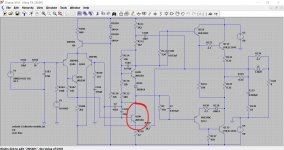
Just to make sure we're talking about the same diode - see snip enclosed.
Attachments
Ah, no we are not 🙂
That one looks like some kind of protection device (Zener) but if it were leaky or anything like that then it would effect the negative going part rather than the positive as it tries to turn off the PNP driver.
If you have any doubts then just snip it out as a test. It shouldn't normally come into play.
Back to it after some time put into a couple of design projects.
Putting notes here as I collect info. Decided to input sines @ 1.4V and trace through signal path. Well, this is weird. Q201(B) already shows the positive part of sine cutoff... Can't imagine why as there's sol little circuitry before it. Tried switching HPF on and off to no difference.
Putting notes here as I collect info. Decided to input sines @ 1.4V and trace through signal path. Well, this is weird. Q201(B) already shows the positive part of sine cutoff... Can't imagine why as there's sol little circuitry before it. Tried switching HPF on and off to no difference.
Last edited:
Back to it after some time put into a couple of design projects.
Putting notes here as I collect info. Decided to input sines @ 1.4V and trace through signal path. Well, this is weird. Q201(B) already shows the positive part of sine cutoff... Can't imagine why as there's sol little circuitry before it. Tried switching HPF on and off to no difference.
Stop press! Was measuring wrong. The amp board has a different symmetry L/R than the older version... But I do think something is amiss with Q201.
Will keep posting my readings.
I'm still here 🙂
I'll try and pick it up again tomorrow but there should be some really quick and simple checks we can do to confirm that the output stage can swing positive.
I'm thinking that if the VAS stage is cut off or removed then the output will swing to the positive rail. That was Q106 in my simulation. Be sure to have NO LOAD attached if you try this.
Attachments
I'm still here
I'll try and pick it up again tomorrow but there should be some really quick and simple checks we can do to confirm that the output stage can swing positive.
I'm thinking that if the VAS stage is cut off or removed then the output will swing to the positive rail. That was Q106 in my simulation. Be sure to have NO LOAD attached if you try this.
I haven't yet looked at this. But some (other) progress below.
After a closer look at the voltage readings of Qs, I realized Q204 was reading 1V Vbe, so I pulled it out (and confirmed it was a mess). But, as I was figuring this out, at this one turn on, R312 and R307 went up in smoke. I thought - either probe slip (but at the current levels those resistors should see... a second of probe slip couldn't have triggered a conflagration), or Q204 was marginal, and I pushed it over the precipice (I was going pretty high up and down signal level to figure the waveform/distortion vs level). It also made some sense, maybe, as signal was being brought up in level, the CCS was being forced off its limits due to a marginal CCS driver, therefore the clipping of the sine from that level on.
Anyway, I replaced it with 2N5401, but I still have a brand new fried R312. I tested Q301/302 after the first frying, and they seem fine. Also fine are Q201-204 (diode test).
I don't know, there's either some sort of short thorough a path in the input stages (Q205/206?...), or Q301/302 exhibit some short (BC), but only under load (though both?...). Q206, for one, shows a bit low Vbe for comfort (0.43V).
I feel trouble lives in the Q205/206 neighborhood. It puzzles me whatever short goes through there can fry a milspec CMF60 (R312), but seems to leave Q301/302 standing. Though maybe I should test those two again. No matter how I look at it, I can't really place the melting PS resistors in the context of fixing the CCS.
I'm thinking:
- Pull out Q205/Q206 and test. Maybe Q105/106, just in case the stink has spread, or just to reduce the variables.
- Disconnect the input stages from PS to see if Q301/302 output expected voltages and R312/307 survive.
BTW, again found signs of previous work. Q202 is a 2SC1364 (Q102 uses the spec'd 2SC632A).
Marching on. Tired tonight, but tomorrow a new day.
Thank you.
It sounds like a lot is going on fault wise.
R307 and 312 would burn if there was an overload on the rails they supply. That said there doesn't look anything capable of doing that looking at what they supply in normal operation.
Looking deeper it is possible you shorted something around Q204. If that happened then there is a possible conductive path from rail to rail via the input transistors and double diode and so all these need checking/replacing together with the low value resistors.
Q301 and Q302 may have suffered, these are just used as ripple filters.
Attachments

It sounds like a lot is going on fault wise.
R307 and 312 would burn if there was an overload on the rails they supply. That said there doesn't look anything capable of doing that looking at what they supply in normal operation.
Looking deeper it is possible you shorted something around Q204. If that happened then there is a possible conductive path from rail to rail via the input transistors and double diode and so all these need checking/replacing together with the low value resistors.
Q301 and Q302 may have suffered, these are just used as ripple filters.
Mystery goes on - tough cookie this one. All the prior signs of work show I'm not the first dealing with it.
Anyway - Q204 was bad (open junctions), replaced with 2N5401. D201 was also taken offline (though brand new 1N914s). Whatever trigger event occurred right before the violent death of the PS resistors (my hypothesis - marginal Q204 going worse, due to tests), shorted Q203 in all ways possible. This was what was keeping the nuclear button actuated on the PS.
Having suspected Q205, I pulled it out, and initial measurements seemed to show it open (so I replaced both channels with MJE340), but later checks show it ok... In my defense, heavily oxidized legs on very old transistors. Vbe was not too good anyway, so I'm fine with it replaced. Mentioning this to keep a log on parts in the actual amp at this time. On that channel, only Q205 stays original at this point, though just tested it again (diode test) and it's ok.
At this point, I have stable voltages into the input stages, but not healthy signal through. Signs at this point:
- both channels output signal, though highly distorted (looking at it in FFT, tall harmonics all across). At least it's at even levels between channels for a given position of the volume controls. This has never happened before with this one, so at least that's some sort of progress 🙄
- I can't adjust the bias on either channel (meaning the pots just don't change the mV on the test points). This is also new, I was able to adjust somewhat to reasonable levels before. Strange this occurs on both channels. I don't think there's common circuitry involved in this. 😕
Mooly - hopefully, I at least keep you entertained... 🙂
My plan is to get up early tomorrow morning and try to hone in the current information on this one unit.
Recap, review what information and facts are gathered and what not, attempt to confirm the knowns and unkowns (ha! proverbially). I think I need to; I feel a good bit lost on mapping this one out, and so I assume it can only be less clear to you and others following this. I do hope I'm making this as seamless, fun and productive as it can be. Thank you for tagging along and helping as much as you do.
The summary above stands though.
Oh yes, its a good read 😀 but difficult at a distance to pick up on all the twists and turns.
I would expect any obvious signal fault to also show as incorrect DC conditions somewhere down the line.
Output offset is always the prime measurement. Then you have your bias current which is it is not adjusting shows a problem.
I wouldn't worry over looking at FFT's, just aim to get a full sine voltage swing at the output initially.
Non adjustable bias comes down to ensuring the voltage across Q105 and its series diode can put enough voltage between the bases of the drivers and outputs.
Its a Quasi stage so needs at least three Vbe's worth to do that, say 2.1V.
Q108, 114, diodes D103 and 110. Pull them all out until its fixed. You don't want to be fighting possible problems with the protection circuitry pulling things down. And of course use a bulb tester in that scenario.
May find it hard to get to the bench as early as I hoped (so I'll parse work here throughout the day as I can), but on a quick note, the highlights of the current condition are:
- DC offset is minimal - R is 22mV, L is -14mV. This has been adjusted prior to recent work (few weeks back).
- Bias cannot be adjusted.
I think Q105/205 should be the focus next, as you point out. Thank you for also for the point on the protection circuitry.
- DC offset is minimal - R is 22mV, L is -14mV. This has been adjusted prior to recent work (few weeks back).
- Bias cannot be adjusted.
I think Q105/205 should be the focus next, as you point out. Thank you for also for the point on the protection circuitry.
If the offset is good then that implies the DC conditions on each driver transistor base will be correct... but check them. You should see approx plus 1.2 volts on Q110 base and approx minus 1.2v or a little less on Q111 base.
Assuming that is good then you need to look at the voltage across Q105 +D102 and also the current flowing in that chain.
So that is the voltage between R113 and R117. This should equal your plus 1.2 and minus 1.2 added together as a total. So 2.4 volts in total and this voltage will vary as you alter the bias preset.
If it reaches and goes over that figure then something fundamental is wrong around the drivers and outputs.
If it adjusts but doesn't reach 2.4v then that is why there is no bias current available. You then need to check the current in the bias chain.
You should have a total of approx 60 volts across R111 and R112. Check it.
Then calculate the current from your measured voltages. Lets say you have 52 volts. That is a current of 52/(2200+4700) which is 7.5 milliamps.
We check that result by measuring the voltage across R118, the 22 ohm in the emitter of the VAS stage. You should see approx 0.0075*22 which is 165mv.
If it falls down at any point then stop and check the resistor values are OK by measuring out of circuit.
Attachments
Mooly,
Below my findings from tonight. Unless specified, values are measured with bias set to minimum (fully CC).
DC offset tonight was a bit wondering, but I don't think it ever exceeded 30mV on either channel.
Base of drivers - Q110: 0.41V; Q111: -0.85V; Q211: -0.3V; Q210: 1.18V. Doesn't look very good, though maybe the state of bias adjustment (min bias)?
For the voltages across the bias set circuitry, I measured like this. Q105c: 0.42V; Q106c: -1.61V; Q206c: -0.32V; Q205c: 1.77V.
To establish capacity to vary the bias voltage, I probed between R113-R117 (essentially, same nodes as just above). I was able to go from 2.05V to 3.24V (!). On the other channel (R213-R217), my range is 2.11V to 3.27V (!). Something stinky seems to be going on with the drivers or outputs.
Just to keep at your points, I measured across R111/112: 62.5V, which renders 9mA through there. I see 239mV over R118, which is a bit different (10.8mA), but not by that much to be worrisome, I don't think (not sure where that current would leak there either). On the other side, R211/212: 61.2V, so 8.8mA. Same calculation over R218 (149.5mV) gives 6.8mA... Again a bit (more) off. Pulled one leg on all those resistors (111, 112, 118, 211, 212, 218), but they measure OK.
Oh, also, I measured 0.02V over D202. I assume there's one junction over that so 0.6V would be expected so maybe that thing is also gone. Didn't look at the other channel for this.
I have not (re)investigated the L transistors on the input (the incident on the PS from the past couple of days may have taken a toll), but I didn't have any red hot flags on there before. I have all input transistors replaced on the R except Q205, but it repeatedly checked ok to diode test so I left alone.
It seems something's going on with the power handling Qs. I will need to double check all Vbes down each chain, it seems to me. And, yes, also need to pull protection circuitry out - it's entirely possible, again, glaring faults are hidden under some clamping.
Last edited:
Interesting set of results. Concentrate on one channel at a time.
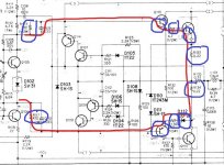
Lets work with the bias voltage that can be swung as high 3v and over. That should take the output stage to destruction and so we need to see why it is not doing so.
If you turn the bias voltage up to the high end (so 3v and over between R113 and R117) can you measure any volt drop across R113 and R117 as that will allow us to deduce the current flowing into the base of the drivers?
There shouldn't really be anything significant across those resistors and consequently only very minimum current in those resistors.
Each half of the output stage is a Darlington configuration with massive current gain and so only a few hundred microamps needs flow in those two resistors.
The 3.2 volts (for example) that you have across the bias generator must be accounted for in the sum of volt drops across the 330 and 470 ohm resistors together with each B-E volt drop and the diode D112. It is a series path from start to finish.
They must add back up to that starting voltage. So something somewhere is dropping more than it should and yet not allowing the output stage to conduct.
Each B-E junction and the diode should clamp firm at no more than around 0.7v which is only 2.8 volts total. In practice the figure would be less because each transistor will begin conduction below that 0.7v level.
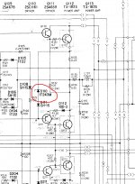
Measure across each item rather than measuring from ground to see that actual voltage. Each volt drop is circled. One of them is likely showing more than it should. Don't discount breaks in the print either.
You could try measuring from the Collector of Q105 (Red meter lead here) and work around the loop. You should see the drops add up as you go around each node.
Hope that makes sense 🙂
Lets work with the bias voltage that can be swung as high 3v and over. That should take the output stage to destruction and so we need to see why it is not doing so.
If you turn the bias voltage up to the high end (so 3v and over between R113 and R117) can you measure any volt drop across R113 and R117 as that will allow us to deduce the current flowing into the base of the drivers?
There shouldn't really be anything significant across those resistors and consequently only very minimum current in those resistors.
Each half of the output stage is a Darlington configuration with massive current gain and so only a few hundred microamps needs flow in those two resistors.
The 3.2 volts (for example) that you have across the bias generator must be accounted for in the sum of volt drops across the 330 and 470 ohm resistors together with each B-E volt drop and the diode D112. It is a series path from start to finish.
They must add back up to that starting voltage. So something somewhere is dropping more than it should and yet not allowing the output stage to conduct.
Each B-E junction and the diode should clamp firm at no more than around 0.7v which is only 2.8 volts total. In practice the figure would be less because each transistor will begin conduction below that 0.7v level.
Measure across each item rather than measuring from ground to see that actual voltage. Each volt drop is circled. One of them is likely showing more than it should. Don't discount breaks in the print either.
You could try measuring from the Collector of Q105 (Red meter lead here) and work around the loop. You should see the drops add up as you go around each node.
Hope that makes sense 🙂
Attachments
I've measured the above (gotta go back on a couple of spots) - but I'm not sure if protections (Q108, Q114, D103, D110 & other side) should disconnected for these measurements to be relevant. Also, what about the Q303 through Q307 part of the circuitry?
I'm getting some pretty weird readings and wonder if it's again the case that the protections are on and messing with the "natural state" of the devices.
I'm getting some pretty weird readings and wonder if it's again the case that the protections are on and messing with the "natural state" of the devices.
You can remove Q114 and Q108 together with either D110 or D111 although I doubt there is a problem here, at least with the transistors because any conduction at that point would tend to lower the bias voltage available... and you have over 3 volts available.
Those diodes though, yes pull either of the two.
Q303 to 307. Again the fact you have 3+ volts available suggests these are not adding to the problem but again, we can be 100% sure by isolating them. Just lift D316 and D317.
It's advisable to make notes of what you do lift as its easy to forget and keep track of 🙂
Given the considerations with the voltage headroom (>3V), I am starting by lifting one leg of D110, D210, D316, D317. Let's see if DC offset or anything else shoots through the roof.
Also, bias set at minimum.
Obviously, all this with bulb tester.
Also, bias set at minimum.
Obviously, all this with bulb tester.
- Home
- Amplifiers
- Solid State
- Sony TA-3200F: huge output DC offset