Found it.
So those diodes effectively clamp (remove) the drive to output stage. It is fine to leave them out for faultfinding.
That is the weirdest protection circuit I have ever seen tbh. An oscillator that is powered by rectifying any polarity of DC offset and then using that to fire a thyristor. Bizarre 😀
Try doing as I suggested, take the LT diagram (or a screen snip of the manual) and add your own measured voltages on all the main transistor nodes. It should start to make sense then.
Did you get the lead polarity of any replacement semis correct? as the 2N devices will be different to the originals.
I'm going to post voltage readings of the faulty R amp as I get a chance to read them. Not a lot of time to digest between them.
So Q204 (SPS885) sits cracked wide open between +59V on the C to -58V on the E. B is at -11.7V. This looks like a perfectly good culprit, though not sure if the cause of the fault. Q205 is at +59V on both B and C, and the E is at +58.6V (so kind of looking fine by itself as BE seems correct).
While I was measuring, C210 popped open, likely seeing far more than the 25V the cap was rated for. I assume C211 is not far behind.
I am not sure yet what's broken here, but any guesses or pointers to what to measure next are welcome. I'm getting bits and pieces of time during parental duty in a quarantined household.
Been checking resistors last night but can't yet find anything glaringly wrong. Plan to finish resistors soon and when all have one leg out will be easier to test the junctions on the transistors.
On the bulb tester. I am aware of it being used to prevent shorted components from flipping breakers or fuses and stuff, but not sure how it's useful for testing the outputs. Run the amp with the bulb in series and examine the 0.5ohm resistors for anything wildly different, indicating an opened or shorted junction on the finals?
Thank you all your for continued support.
I sometimes resort to leaving outputs out of circuit and route driver stgae back into ltp. That leaves me with a circuit that shouldnt blow fuses.
You can then check for sensible voltages.
You can check the whole circuit without every powering it up by checking individual components. A pain if its a complicated amp but a simple is easy to check.
A good precheck is just a very careful visual inspection for cracked components, cold solder joints and burnt/broken tracks.
Mooly - are you sure 2N5550 is up to duty as Q204? The sim shows dissipation to be at about 830mW, while 2N5550 is rated for 625mW.
My amp has an SPS885 there, which I can't find data on, but it's on a TO202 or whatever this is, and I assume can handle some 100s mWatts without heatsink.
My running assumption right now is that Q204 has its C open and that makes no current be drawn through all those resistors to B+ and that lifts all that side up to the almost +60V I am seeing. Not sure what to replace it with to verify this assumption, as 2N5550 seems too flimsy for that position.
Last edited:
In the sim, running R217 through its entire range (with default values for those resistors), I am getting between about 577 and 833mW on Q204, all too high for comfort for a max absolute of 625mW, I'd say.
I'll be looking at whether MJE340 is a good choice for that position.
I'll be looking at whether MJE340 is a good choice for that position.
Last edited:
Jackpot!
Got it figured! 😀😀😀
Q204 was busted. Output was shooting to B+ DC-wise in the right channel, and that was triggering the speakers protection. The later was obscuring all behaviors (including seeming to point to both channels being faulty). Quirky protection system for sure... In retrospect, I looked at disabling this early on, but other scenarios came to front burner and so it is. Happy camper never the less.
BTW - MJE340 works well there. Replaced both channels for good measure and symmetry. 2N5401s work well, also, on the inputs.
As far as your sim goes, Mooly - your OP was different, so 2N5550 was a good fit there. Not in this case though, so my extrapolation was not warranted. I wouldn't have known that without LTSpice, so thank you again for that tutorial!
Bias adjusts now to less than 1mA from 25mA, and very steady, and DC on output is (much) less than 1mV, and also very steady. This is with the new pots, which gives me a lot of reassurance (sleep factor from brand new, encapsulated pots).
Well done  and there do seem to be a few different versions of this around.
Worst case Q104 (204) could see the total rail voltage (- and + added) if the output swings toward one or other rail. MJE's are a good favourite, they been around for decades.
Excellent 🙂
and there do seem to be a few different versions of this around.Worst case Q104 (204) could see the total rail voltage (- and + added) if the output swings toward one or other rail. MJE's are a good favourite, they been around for decades.
Excellent 🙂
Definitely feels good to have this running again. Late night here, but tomorrow I'll give it a good whirl in my rack and I'm pretty sure it will take my Thiels out to town 😉... Success this far is being reported off of AP box readings and other bench measurements.
Now, on to the other sample I have here. This one's of the newer variety (no separate speaker protection board). Fully recapped, it gives me pretty high distortion with both signal in and load on the outputs. Also, given the above, it lights the dim bulb fixture. It gives me reasonable readings on AP frequency response tests even under these circumstances. Distortion readings are in the weeds though.
With no load and signal, I could bias it appropriately and get it to <1mV DC on outputs. Will investigate it further tomorrow.
Early morning here 🙂 Not had breakfast yet.
Remember that the bulb tester will drop the rail voltage a little (and a lot under load) and so any final bias adjustments must be done on full mains once you are sure all is well.
Distortion probably would be high in such a case.
I can't get over that protection scheme, truly bizarre of whoever dreamed that one up.
In the middle of "re-resistoring" (ha!) the second unit. I have been replacing with CMF55/RN55 or higher rating, as needed, everywhere. Sony though, has been specifying carbon, and composition, in addition to applicable power ratings, on various spots. Obviously, the thinking there may be temperature coeficients and all that behavior.
I am curious of thoughts on how much I should worry about that / stick with the resistor material based upon those considerations (or any other meaningful angles).
I am curious of thoughts on how much I should worry about that / stick with the resistor material based upon those considerations (or any other meaningful angles).
Nothing in the amp will use or rely on the tempco of a resistor.
I wouldn't like to second guess a reason beyond saying they are used in non critical locations and might save a fraction of a penny... and those old 5% original parts are pretty decent quality in the scheme of things.
I wouldn't replace any of those 'just because you can' 😉 Keep the originality.
I wouldn't like to second guess a reason beyond saying they are used in non critical locations and might save a fraction of a penny... and those old 5% original parts are pretty decent quality in the scheme of things.
I wouldn't replace any of those 'just because you can' 😉 Keep the originality.
Thank you, Mooly. Agreed.
Any experience with replacing the power transistors? I tried to pry one out last night and it's either heavily oxidized in place or soldered on its socket. The latter would be a painful. Not sure what others have seen with these.
Not sure I need to replace but would like to figure out a more convenient way to test. ON the previous one I unsoldered the GRN, GRY, etc wires coming to the board and main caps.
The old thermal paste can literally stick like glue sometimes but unless they are fried there is no need to replace them. 99.9% of failures in output devices are normally definite and usually C to E shorts.
Replacing old with modern parts (particularly drivers as well as outputs) can sometimes need other tweaks in the circuit to ensure stability and also occasionally to ensure that the bias control works within its intended range due to slightly different doping processes giving a different forward Vbe voltage.
Replacing old with modern parts (particularly drivers as well as outputs) can sometimes need other tweaks in the circuit to ensure stability and also occasionally to ensure that the bias control works within its intended range due to slightly different doping processes giving a different forward Vbe voltage.
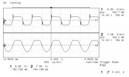
Here's what I'm getting out of this at this point. See enclosed waveform from scope. 1 is R and 2 is L. I input 1.4V RMS 1kHz tone out of AP box. 8ohm loads attached to outputs.
- R: not much useful output coming out, highly distorted, and not exceeding a few tens of mV regardless of volume controls.
- L: Positive part of sine becomes cutoff around a bit past 2V out (was reaching for 2.8V RMS for 1W measurements). This seems to indicate to me one side of PP is broken.
- R: not much useful output coming out, highly distorted, and not exceeding a few tens of mV regardless of volume controls.
- L: Positive part of sine becomes cutoff around a bit past 2V out (was reaching for 2.8V RMS for 1W measurements). This seems to indicate to me one side of PP is broken.
Attachments
So... just enlighten me then because a month is like a zillion posts back in time for me.
You fixed the first amp, that's all done and OK and this is a second one?
As there were different versions it would help if you can post the relevant diagram for this version 🙂
Three basic checks that tell us much are:
1/ That DC offset is zero.
2/ That the bias current is adjustable and able to be set to the recommended value. That tells a lot with regard to current flow in the VAS stages and bias generator.
3/ That the applied input signal is clean when viewed on the scope and that it reaches the input stage correctly i.e. no soft muting at the front end of the power amp causing issues.
4/ And always confirm all supplies are correct at their destinations.
The clipped sine indicates a problem with the upper half of the output stage. Even something as simple as the resistive feed supplying the VAS stage going high in value could cause that... the two series resistors the bootstrap cap connects to.
Also if there were a break in the print (or OC resistor) from the driver to the upper output transistor base or the upper 0.22 ohm being open.
Its very rare to get an open circuit power transistor but I suppose it has to be considered although DC voltage checks would prove that.
So... just enlighten me then because a month is like a zillion posts back in time for me.
Mooly - yes, sorry if I'm making this confusing. See below.
You fixed the first amp, that's all done and OK and this is a second one?
Yes, indeed 🙂
As there were different versions it would help if you can post the relevant diagram for this version 🙂
This one corresponds with the later service manual. For instance, the differential pair is supplied via a CCS. It's pretty close to the configuration you shared your spice for.
Three basic checks that tell us much are:
1/ That DC offset is zero.
Very close, and adjustable OK apparently.
2/ That the bias current is adjustable and able to be set to the recommended value. That tells a lot with regard to current flow in the VAS stages and bias generator.
Well, this is where things get a bit interesting:
L: After figuring a disconnected wire the bias got adjustable to about 20mV full scale. After running for a while - time spent measuring other voltages - I noticed it creeped up to abput 30mV and adjusted to 25.
R: Would get to about 6mV or maybe further but under 10mV depending on conditions (adjustment inertia, warming up, etc.).
3/ That the applied input signal is clean when viewed on the scope and that it reaches the input stage correctly i.e. no soft muting at the front end of the power amp causing issues.
Not sure exactly where you're heading here. I think you ask whether I've scoped the signal through the input stages to see if there's clipping or other early damage to the signal as it travels through the amp. I haven't done this.
4/ And always confirm all supplies are correct at their destinations.
Haven't seen anything out of order here. Also, DC operating points on transistors show no red flags this far... But I haven't checked them all. And none out of circuit.
The clipped sine indicates a problem with the upper half of the output stage.
This is where I was heading too.
Even something as simple as the resistive feed supplying the VAS stage going high in value could cause that... the two series resistors the bootstrap cap connects to.
I've gone full monty on the resistors and so, unless I made a mistake, they should be solid.
Also if there were a break in the print (or OC resistor) from the driver to the upper output transistor base or the upper 0.22 ohm being open.
Checked the 0.22 Rs and they all show continuity. With what I have at hand, it's hard to measure actual values for such low resistance parts though.
Its very rare to get an open circuit power transistor but I suppose it has to be considered although DC voltage checks would prove that.
Will persist in mapping out the voltage chart.
Thank you, Mooly.
^ Thanks. A lot of the checks are simply to make sure we overlook nothing. Never assume anything is OK until it is proved to be so.
So the basic readings all seem OK so we need to look a bit further.
A good check is to place your meter negative lead on the output node (junction of the 0.22 ohms) and work forward looking at DC voltages.
Try and set the bias so that at least there is 'something' flowing and then measure the voltage on the base of the upper NPN output. It should be around 0.6v Now move to the base of the driver. You should see another 0.6v added, so 1.2v in total.
If the upper NPN driver was very low gain or had a B-E short but otherwise OK it would also give you the effect you have of a clipped sine. That might be worth looking at although those two voltage checks should reveal an issue like that.
Try and set the bias so that at least there is 'something' flowing and then measure the voltage on the base of the upper NPN output. It should be around 0.6v Now move to the base of the driver. You should see another 0.6v added, so 1.2v in total.
I've checked all signal path transistors voltages last night and I don't see any glaring red flags on either channel. To your point above, here are voltages on B:
- Q212: .6V; Q210: 1.17V
- Q213: -59.5V; Q211: -1.25V (this is the cuasi-complimentary side. I go by service manual transistor numbers, bottom to top)
- Q113: -59.3V; Q111: -1.21V (same as right above)
- Q112: 0.61V; Q110: 1.18V.
For all these, Vbe's are between 0.4V (Q213) and 0.58V (Q112 and 212). The 0.4V is a bit odd, all others are above 0.53V (Q111). Hey, what do you know, I almost put them all on here! 🙂
The only thing that really irks me is Q205: Vb is 0.53V, Ve -.13V, Vc 1.72V. Vb is positive while the sim wants it negative (-686mV). Being relative to where I'm grabbing my ground (- of C317), it may just be OK. Another possible oddity is how close to zero the finals legs that "sit" on the 0.22ohms are. All four read between 0.000V and 0.03V. The sim wants them at about 0.4V. I'm thinking due to this being idle, very little current flows through the 0.22s and so very little "lift" of those legs from zero.
To keep apples with apples - Q2XY are R, Q1XY are L. L is the better working channel, with the clipped positive half.
The simulation is very critical on the models used and the bias that those models give.
I've had to use a 1N5158 (standard library model) for D102 to get the current low enough in the 0.22's. Currently running 50ma bias current.
Anyhow your voltages on the upper NPN side look fine.
Q211 base looks good.
The lower NPN output can't really have Vb measured as we are doing because it is referenced to the negative rail. You need to just go across R137 to read that but 0.4 actually looks OK and would be typical of the Vbe of old devices made using slightly different process to those we use now.
Q205 looks OK as well. The voltages here aren't quite so clearly cut because the collector will be around 2Vbe drops above the output line (the two upper NPN's) and the emitter and its diode will only need be around 1 Vbe drop below the output line because the lower section of the output stage only has one Vbe drop to overcome (although we do have D112 in there). The lower NPN Vbe drop isn't in that series 'loop'.
Which all gets us no nearer 🙂 The positive clipping is a problem in the upper half of the stage.
OK, so we have to look at the theory and the two upper NPN's form a Darlington which should have tons of current delivery available.
Provided R111 and R112 are OK then I'd guess that something is amiss with one of those transistors. If all the interconnecting paths are good and the 4.7 ohm and 330 ohm base resistors are good then I think we have to try different devices in those locations to prove/disprove the theory.
If you fit different parts be sure to set the bias to minimum first... even going to the point of also linking out D102 to make sure the bias control voltage gets low enough for zero bias with any new parts.
Always best to use a bulb tester as well when doing work like this.
- Home
- Amplifiers
- Solid State
- Sony TA-3200F: huge output DC offset