hey guys just to let you know the PCB orders are only for personal use not for profit I'm just saying no group buy or anything like that, all is me just having fun that all 🙂
Vargas
Vargas

Vargas
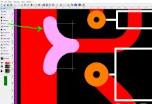
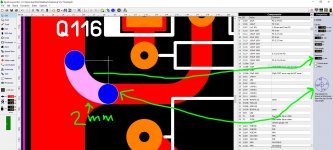
That is a nice pcb. I've been wondering how you're making those nice rounded internal corners on the tracks coming in from the power rails? Rudi used them a lot on his Black Beauty. Are they fill zones?
OK. Thank You!
Regards,
Sumesh
Regards,
Sumesh
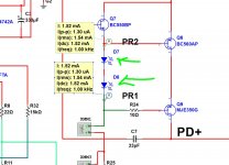
Since Spooky is cascoded a lower Vceo pair can be used (1015/1815).
992/1845 needs to be used for the cascode since it sees full rail.
For the spooky , any >30v pair can be used , comp. pair only sees 12V.
OS
That is a nice pcb. I've been wondering how you're making those nice rounded internal corners on the tracks coming in from the power rails? Rudi used them a lot on his Black Beauty. Are they fill zones?
rounded internals? can you mark what it is? 🙂
Vargas
rounded internals? can you mark what it is? 🙂 Vargas
Hi Vargas, yes I ringed them in yellow on the board attached.
Attachments

Hi Vargas, yes I ringed them in yellow on the board attached.
Those are partial arcs of circles, setting the beginning and ending degrees overlaying traces.
is a circle simple shape
Vargas
oh yes that is easy I use circle and edit to have this fancy shape and grid set to 0.25 and 0.025 mm the circler is 6.50 mm and 2 mm in thickness 🙂Hi Vargas, yes I ringed them in yellow on the board attached.
Vargas
Attachments
Last edited:
Super Great explanation. Those IPS look Super Great too. Hope that the hot SMDs macros can be made with some shapes that use the pcb as a heat sink, especially for the drivers. Great work all the way round.
I still have not figured out how Alex MM did the inverse printing on some of his boards. I will try to post an example.
I still have not figured out how Alex MM did the inverse printing on some of his boards. I will try to post an example.
oh yes that is easy I use circle and edit to have this fancy shape and grid set to 0.25 and 0.025 mm the circler is 6.50 mm and 2 mm in thickness 🙂
Vargas
Got it. Thanks to all.
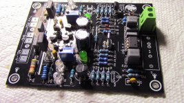
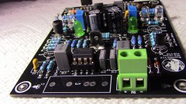
Greenamp v1.2 PCB V1.0 96%
hello guys this is what I got so far I have to take a break this really drain my energy making sure all parts are correct also my back does not help that much 😛
Vargas
hello guys this is what I got so far I have to take a break this really drain my energy making sure all parts are correct also my back does not help that much 😛
Vargas
Attachments
Vargas
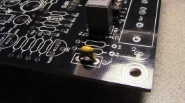
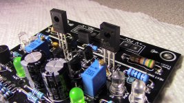
Beautiful. Work of art. I read somewhere recently that LEDs should not be seated flat on a pcb coz it makes them fail prematurely?
Beautiful. Work of art. I read somewhere recently that LEDs should not be seated flat on a pcb coz it makes them fail prematurely?
that is weird I never read that from any forum is a first then I studied electronics in the US Army and I never see that info on any TM anyway I'll check that out why not right? 🙂
Vargas
Different manufacturers will give you different warnings about there LEDs. Some state lifespan is shortened if they aren't driven at full current too.
Different manufacturers will give you different warnings about there LEDs. Some state lifespan is shortened if they aren't driven at full current too.
Yes. It was a manufacturer's datasheet where I came across it when I was looking for pitch data.
Yes. It was a manufacturer's datasheet where I came across it when I was looking for pitch data.
It was the Kingbright 3mm LED datasheet I was thinking of, which recommended a min 2mm standoff. I guess other manufacturers will spec differently as JW says.
http://www.farnell.com/datasheets/1655902.pdf
I was reading the data sheet and I don't see any sentence that recomenended a 2 mm standoff? I know English is my second language what I understand is this sentence that said: "Mantain a minimum of 2mm clearance between the base of the LED lens and the first lead bend" and 2mm spacer? I don't think refers to a actual spacer is about a step before bending the leds I guess?
Vargas
Vargas
I was reading the data sheet and I don't see any sentence that recomenended a 2 mm standoff? I know English is my second language what I understand is this sentence that said: "Mantain a minimum of 2mm clearance between the base of the LED lens and the first lead bend" and 2mm spacer? I don't think refers to a actual spacer is about a step before bending the leds I guess?
Vargas
No prob. I didn't mean an actual 2mm standoff - my bad. I meant a 2mm gap or space. In my own vernacular I call these standoffs, as in 'it stands off the pcb'. I shall consider myself rebuked and stop using my own sloppy vernacular henceforth . In the UK we call this type of manual 'chinglish'. I get where you're coming from with para 4. However, para 3. is unequivocal when it says use standoffs or spacers to securely position the led above the pcb. Fig 3. & fig 4. clearly show unformed led leads spaced off the pcb, (by rather more than 2mm). Para 4. is confusing as it may only be referring to minimum bend radius not to break the led internally. But it equally mght be referring to a convection gap or both. It's not clear. But since para 3. says to space off the led and shows an unformed led I ask myself what would be the point in spacing off less than that, you might as well not space off, but para 3 says you should space off!
When I get to doing mine I shall space off as an insurance policy so I don't mislead myself into fault finding when there's simply a burned out led on board if you see what I mean.
Edit: I'm sure you would only need actual spacers to aid equal height positioning during soldering if you're unsure of your soldering skills. A bit of blue-tak, or whatever, would do the same obviously.
Last edited:
- Home
- Amplifiers
- Solid State
- Slewmaster - CFA vs. VFA "Rumble"