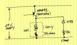
If you approximate the distributed RL nature of the real solenoid, by a lumped equivalent circuit having a single R and a single L, ...
then most of the energy in the flyback pulse is dissipated by the resistor, not by an ordinary flyback PN diode.
To get significantly sped-up turnoff, the external terminals of the solenoid must be clamped at a voltage significantly greater than the rated coil voltage, so there's significantly more voltage dropped across the clamp than across the coil resistance. For a 24V coil, something like a 75V zener and a switching transistor rated Vcemax > 120 volts. Or just a simple resistor whose resistance is 3X the coil resistance.
If you mess with it in simulation, you'll probably also see some lightly damped ringing in the series RLC circuit, at the instant when the voltage across the clamp falls below the clamp's on voltage. The "C" is contributed by the two semiconductors, and is only a small number of picofards. But that's plenty enough for SPICE.
_
Attachments
John would you post a pix of your constant current mod so I can get an idea of where and how you installed it on the board?
Thanks
Alex
Hi Alex,
I'm away from home at the moment but will give a full run down of the mod including how it is inserted in the board over the next weekend. This mod allowed me to completely remove the three diodes D22-24 so no bypass cap needed with its LF cutoff issues. I noticed an improvement to the sound but I would wouldn't I!😉
There is enough voltage headroom in the T2 to allow the cascoding of Q21, possibly with reference to its emitter rather than ground. This will help the linearity of the gain stage a little but I doubt it will have a significant effect on Tom's findings, perhaps more trouble than it is worth? What do others think?
John
Here is an example (certainly not optimal) of fast mute relay driver suited to a DC supply (like the wall-wart intended for this project):
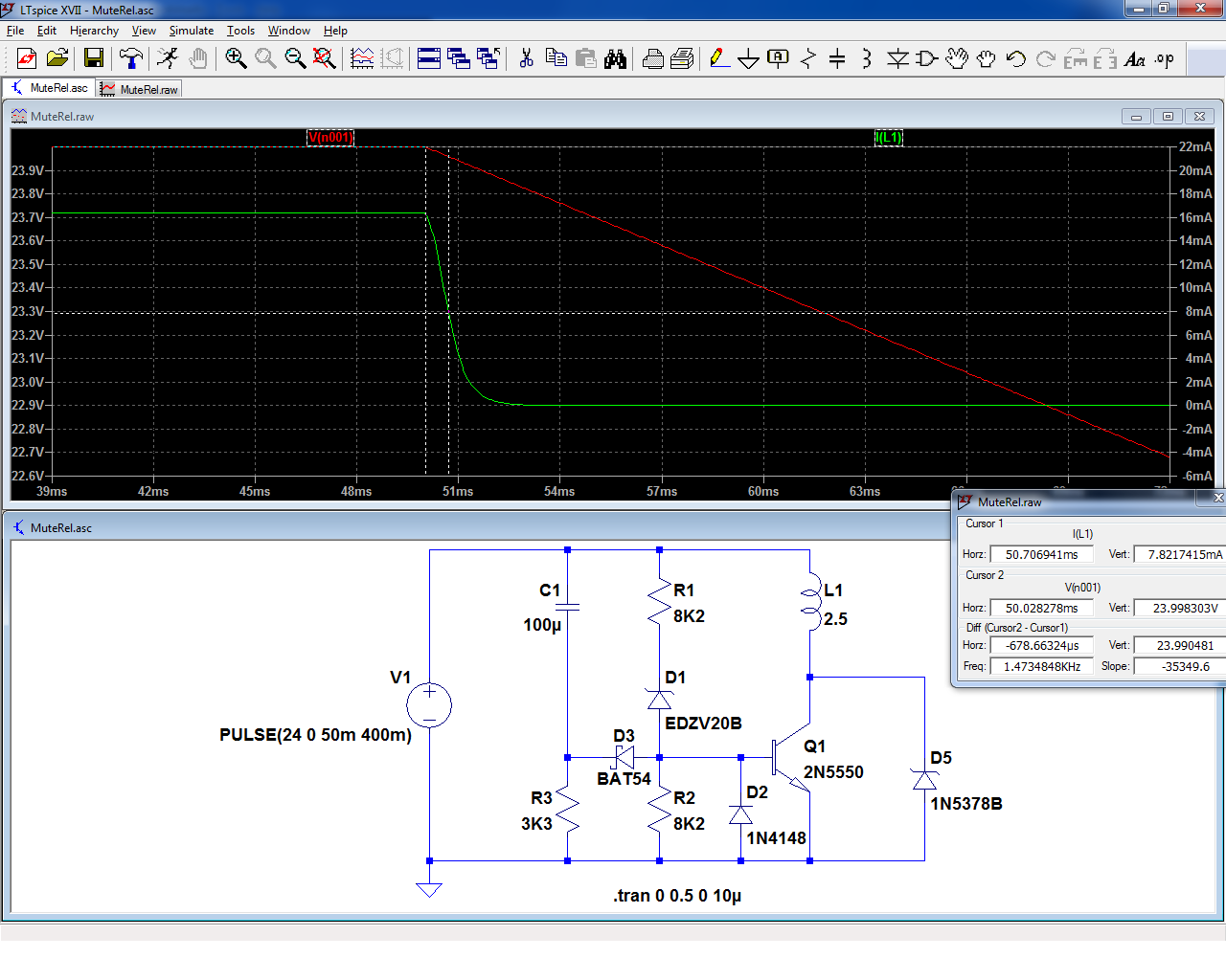
With the half-realistic values picked for the example, the current turn-off time is about 700µs.
The actual reaction time will be several times longer, due to the mechanical inertia of the moving parts of the relay.
This very basic project stub could certainly be vastly improved, by refining the values, or including hysteresis: this circuit assumes a relatively clean turn-off, without too much stuttering.
The example relay is a 1.5K, 24V electromechanical relay, but it could be replaced with a photovoltaic relay with a suitable limiting resistor
Attachments
To put things in perspective, here are the results of a surge on a real VC.
Data. Awesome! Thanks for sharing.
I certainly do not advise going to the limits, but the effect of a limited thump on headphones is probably going to be benign.
I would be more concerned about the eardrums in fact: the turn-off event looks rather nasty, and with efficient HP, it could be problematic
I suspect the smaller and more efficient drivers in IEMs wouldn't take lightly to the thumps either. And good point with the eardrums too.
Tom
Member
Joined 2009
Paid Member
Forget using an old-fashioned relay, it makes no sense they’re bulky they’re not that reliable when facing an inductive load at high current - when I say “relay” I mean solid-state relay, a pair of N-FET’s
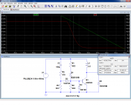
The values I used in my mute relay example were perhaps too extreme, too speed-oriented.
It should work with a good supply, but if the regulation is poor or the output unclean, it will mute when there is no reason too.
In this example, the values will result in a more placid behavior, meaning a longer reaction time, but no overreaction.
Now the time is 2.7ms, but this is with a supply fall rate of 400ms/24V, and by 2.7ms, the voltage is still at 23.84V, which is not too bad (and should be OK in practice)
With R4, it is possible to adjust the reactivity (higher value= less reactivity)
Attachments
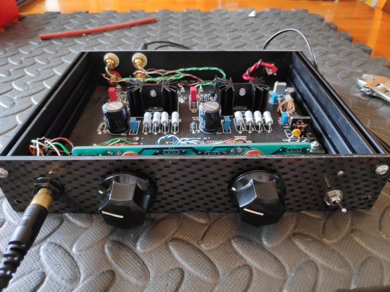
Need a bit of help troubleshooting the power on LED I managed to fry mine by hooking up the power on switch and led switch round the wrong way 😀
I now have 21v on across the led pad so probably need to identify and change out some parts to be able to install a new led.
On the positive side I quickly discovered what was wrong. (need a face palm icon)
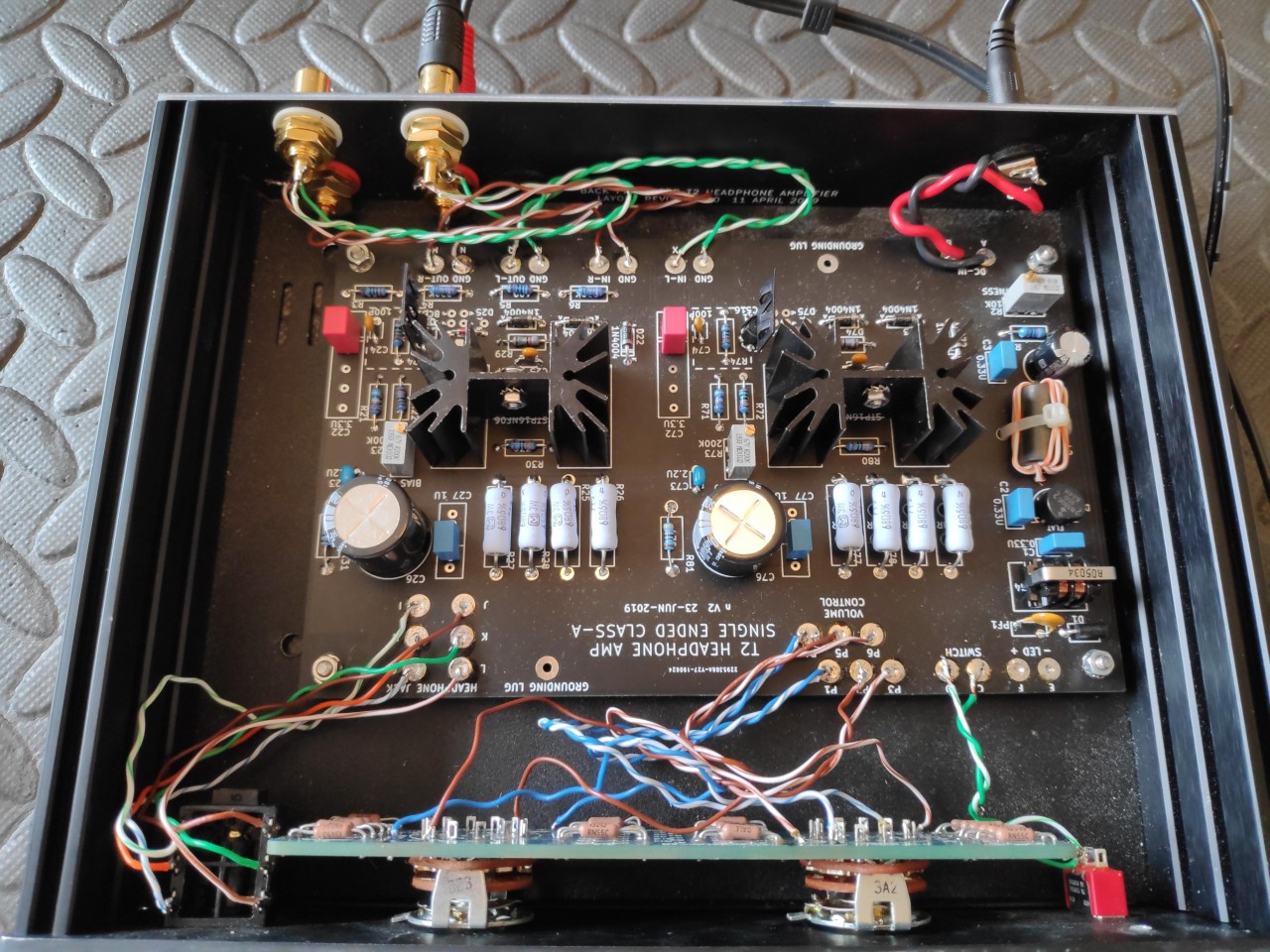
Both channels were subsequently biased to 5.10v.
I checked dc offsets on the headphone jack which were low and plugged some old phones in. The amp side is working nicely and am enjoying listening to some tunes while I type 🙂
I now have 21v on across the led pad so probably need to identify and change out some parts to be able to install a new led.
On the positive side I quickly discovered what was wrong. (need a face palm icon)
Both channels were subsequently biased to 5.10v.
I checked dc offsets on the headphone jack which were low and plugged some old phones in. The amp side is working nicely and am enjoying listening to some tunes while I type 🙂
Last edited:
Glad to see such constructive discussions on how to improve the turn on/off characteristics of this amp.
So I finally got to sit down with the amp and can confirm:
* My build has a mild turn on thump that I never really paid attention to.
* I seem to have had a habit of taking the headphones off (upon hearing the kids wake up or something), then get drawn away from the amp and hit the 'off' button on my way out of the room. Consequently I never heard the..
* Pretty decent power off kick to the eardrums. Enough for me to ensure I disconnect the headphones before I power off.
I'm using 38 Ohm headphones, so the turn on wasn't too bad but the turn off isn't pleasant now I've heard it.
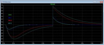
I ran the 'Pulse' command into my earlier spice simulation with a .step command for the most common impedances. It follows Elvee's pretty closely, although I simulated for a 22v supply because the PSU eats a couple of the volts before it reaches the rails.

So I finally got to sit down with the amp and can confirm:
* My build has a mild turn on thump that I never really paid attention to.
* I seem to have had a habit of taking the headphones off (upon hearing the kids wake up or something), then get drawn away from the amp and hit the 'off' button on my way out of the room. Consequently I never heard the..
* Pretty decent power off kick to the eardrums. Enough for me to ensure I disconnect the headphones before I power off.
I'm using 38 Ohm headphones, so the turn on wasn't too bad but the turn off isn't pleasant now I've heard it.
I ran the 'Pulse' command into my earlier spice simulation with a .step command for the most common impedances. It follows Elvee's pretty closely, although I simulated for a 22v supply because the PSU eats a couple of the volts before it reaches the rails.
Attachments
Member
Joined 2009
Paid Member

I was thinking: one option to avoid power off noises without any changes to the pcb is to use an on-off switch with an extra pair of contacts. Wire the headphone output through the extra contacts - when you switch off the power you immediately disconnect the headphones.
Need a bit of help troubleshooting the power on LED I managed to fry mine by hooking up the power on switch and led switch round the wrong way 😀
I now have 21v on across the led pad so probably need to identify and change out some parts to be able to install a new led.
I cheated and used a bi-directional LED.. I just had a lucky dip for the colour 😉
21V across the pads I think is ok as you are basically measuring the rail voltage without an LED connected. With the power off, measure your 820 ohm resistor (R7) to ensure it is still in the region and unaffected.
Then (with the power still off), measure the resistance between GND and LED Anode. Turn the multi-turn pot (R2) until you get a fairly high resistance (10K + 820). This limits the amount of current that may flow through the LED (your brightness control).
Then with a replacement LED correctly oriented, power on and hopefully there will be light 🙂 adjust the pot to suit.
If you want to spec the LED properly, use the digi-key calculator here: LED Series Resistor Calculator | DigiKey Electronics
Just feed it with the rail voltage (21-22V), the LED forward voltage and current (from the spec sheet of your LED) and that will give you a minimum value for R7 (it will be pretty close).
Good luck!
Thanks have ordered some replacement leds.
I was thinking: one option to avoid power off noises without any changes to the pcb is to use an on-off switch with an extra pair of contacts. Wire the headphone output through the extra contacts - when you switch off the power you immediately disconnect the headphones.
Perhaps you're thinking of something along the lines of this part# at Mouser? It ends with an "H" so you get lockwashers and mounting nuts in the package.
_
Attachments
A very simple way to prevent turn on thump is to use a cap multiplier to slowly ramp up the voltage over several seconds. This can be added between the wall DC supply and the amp DC input. Simple single MOSFET and a couple of resistors and caps can be dead-bugged to do this or use a premade cap Mx module. The cap Mx drops 4v though so use a higher voltage wall wart or a dc-dc step up before the cap Mx.
xrk971,
Is this a device that can be purchased and used ?
Alex
There are many muting circuits that can be purchased. Pete Millett makes one and AMB audio makes one too. If you do a google search you can find where to order their PCBs from. 🙂
Thanks !
Alex
Pete Milletts implementation uses a 555 timer which flashes the pilot LED while muting then the LED is on solid when the amp is fully working. Quite neat.
Forget using an old-fashioned relay, it makes no sense they’re bulky they’re not that reliable when facing an inductive load at high current
All true. But the current in a headphone amp is not all that high, so I wouldn't worry too much about the contacts vaporizing.
Relays don't need to be bulky. Some are only slightly larger than the two power MOS you'll need for the switch.
Tom
Tom has raised another, relatively minor potential issue: the behavior on capacitive loads.
Since the cure looks relatively easy, here are some possible leads to address this issue.
This is just food for thought: my sim is grossly inaccurate as I don't have the correct models, and the actual implementation will in part depend on the physical configuration, but armed with this knowledge, DIYers can improve matters.
Here is the problem identified by Tom: my sim may not be accurate, but at least it shows something.
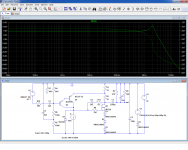
I used an AC sim, because it is simpler and lighter than a transient + squarewave, and provides the same information in a different form, for small signal at least:
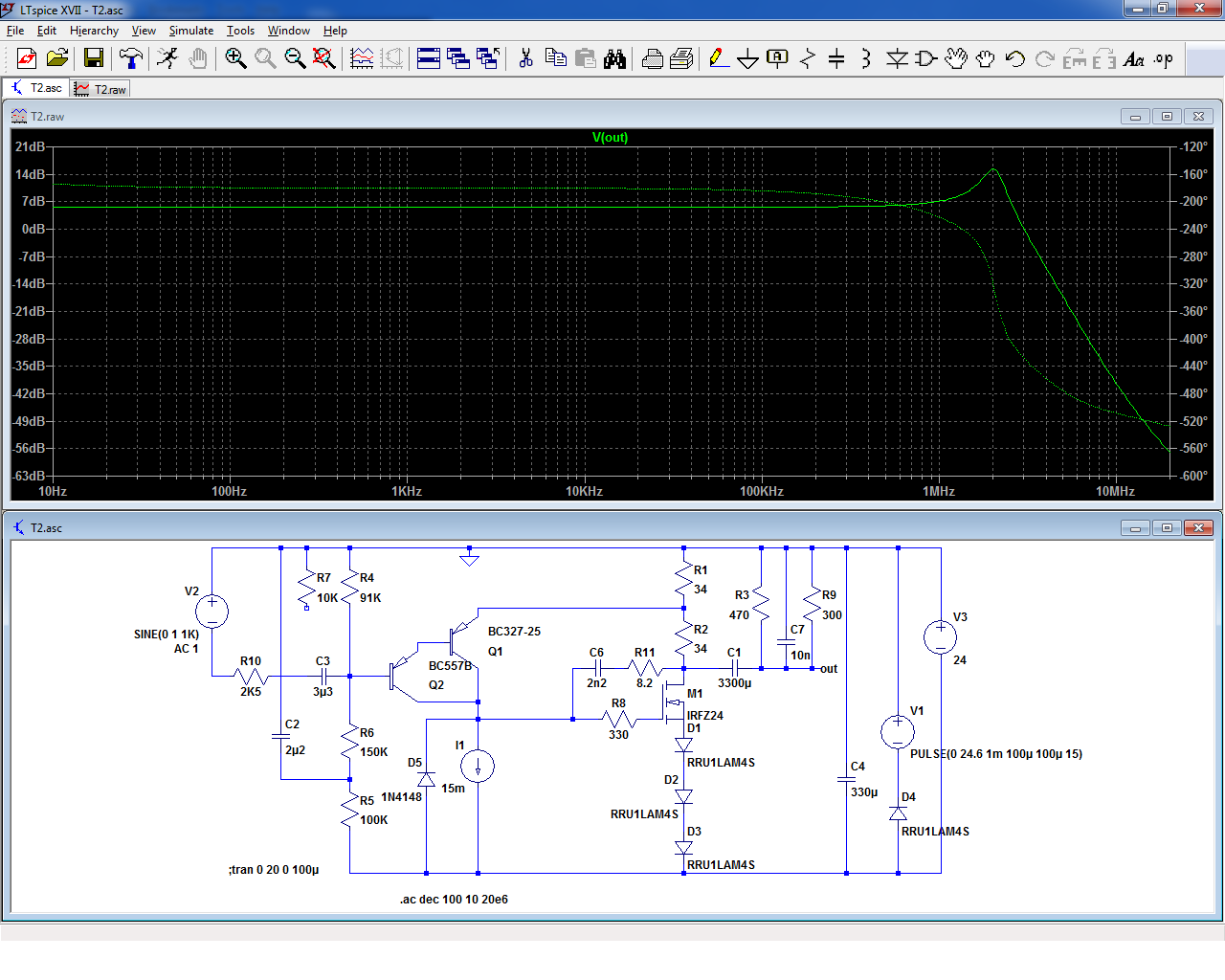
With a capacitive load, a hump is visible: this would translate into ringing in the time-domain.
What are the possible culprits?
One is very obvious: it is the (misnamed) gate stopper:
it adds a pole in the response, reducing the phase margin.
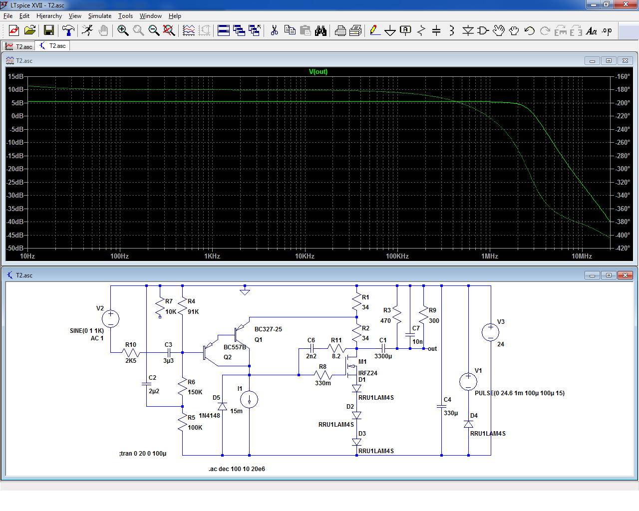
If it is eliminated, by making it 330m, the hump is magically polished off:
There is another, much less obvious perpetrator.
The design heavily relies on FB, because the OL gain is high, and the closed loop gain only 2.
This means that the feedback has an overwhelming influence on the behavior of the amplifier.
The feedback is through the darlington Q1-Q2, operating in common-base from a FB perspective.
To properly operate, a common base stage needs to have its base firmly held at a zero AC potential.
Here, the base has its potential held by the volume pot, symbolized by R10 (pot midway).
For low frequencies, that's perfectly OK, but at higher frequencies, the path to GND is not deterministic: it will depend on wiring, parasitics of the components, PCB, etc.
If this potential is influenced, it will generate anomalies in the closed loop response.
The solution is to ensure a good HF AC ground there, with a small cap having no influence on the LF behavior (C5):
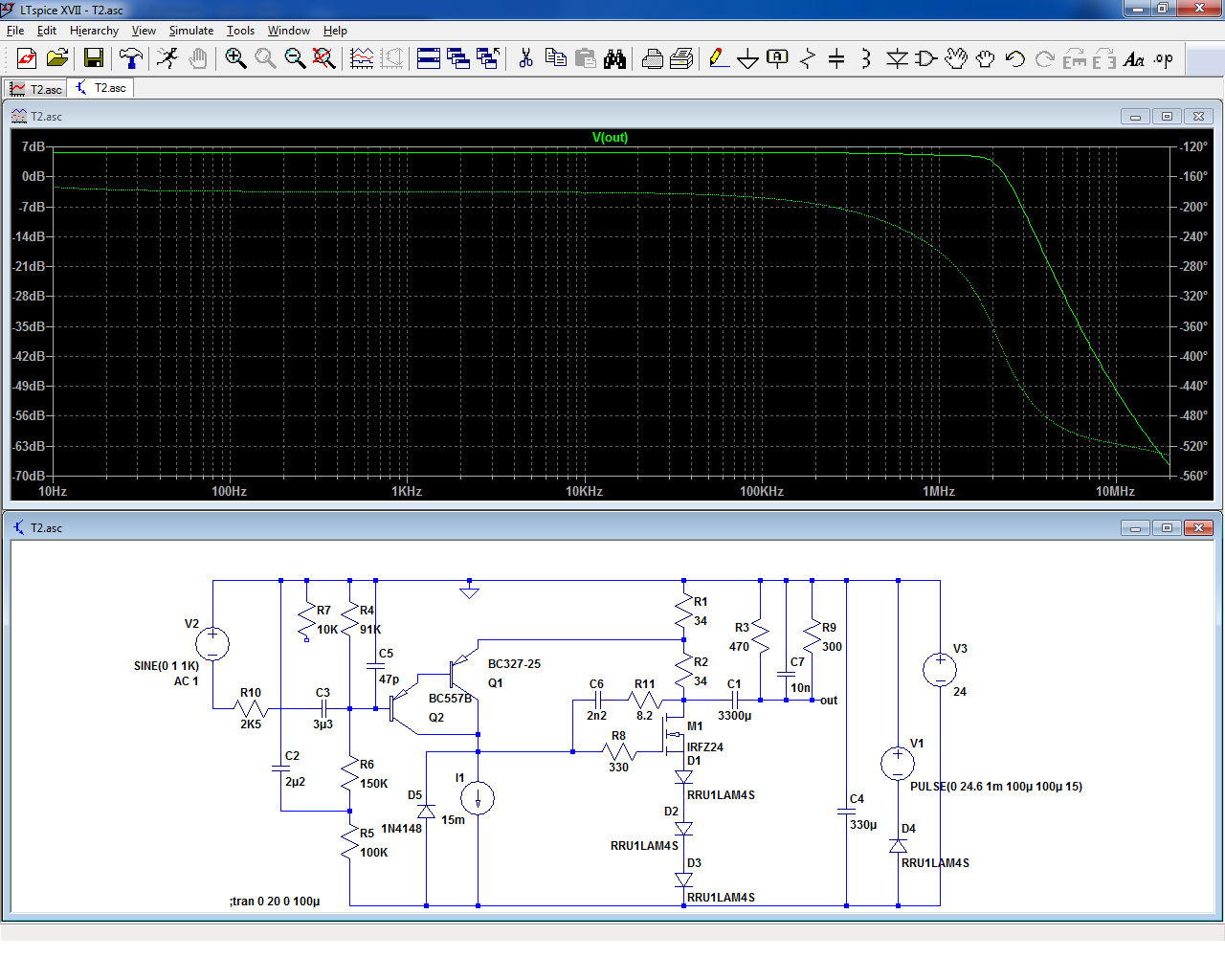
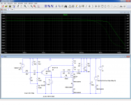
The gate stopper is returned to 330 ohm, yet the hump has also disappeared.
Can both be combined?
Yes, the effect is additive, here the FR with a load increased to 100nF:
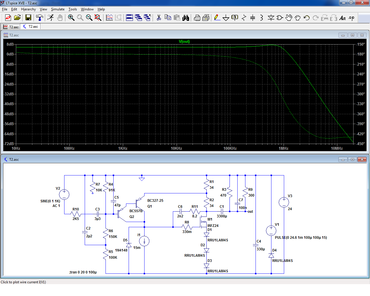
A hump has reappeared, but it is barely noticeable.
Is it safe to dispense with the gate stopper? In principle, yes (very much depends on the layout), and if the compensation network C6 R11 is close enough, there shouldn't be problems.
Will this translate into large/signal, transient, reality?
Not litterally: as I said, the sim is crude, but it provides useful hints at what needs to be done.
Note that since the stability should be greatly increased, the compensation could be less heavy-handed, leading to better/more symetrical SR performance.
One could also consider other compensation strategies: shunt for example, as it would also contribute to SR symetry.
These are just ideas, that need to explored and tested carefully before an actual implementation becomes possible. I cannot go further without using more accurate simulation models, it would be wasted
Since the cure looks relatively easy, here are some possible leads to address this issue.
This is just food for thought: my sim is grossly inaccurate as I don't have the correct models, and the actual implementation will in part depend on the physical configuration, but armed with this knowledge, DIYers can improve matters.
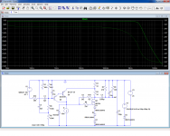
Here is the problem identified by Tom: my sim may not be accurate, but at least it shows something.
I used an AC sim, because it is simpler and lighter than a transient + squarewave, and provides the same information in a different form, for small signal at least:
With a capacitive load, a hump is visible: this would translate into ringing in the time-domain.
What are the possible culprits?
One is very obvious: it is the (misnamed) gate stopper:
it adds a pole in the response, reducing the phase margin.
If it is eliminated, by making it 330m, the hump is magically polished off:
There is another, much less obvious perpetrator.
The design heavily relies on FB, because the OL gain is high, and the closed loop gain only 2.
This means that the feedback has an overwhelming influence on the behavior of the amplifier.
The feedback is through the darlington Q1-Q2, operating in common-base from a FB perspective.
To properly operate, a common base stage needs to have its base firmly held at a zero AC potential.
Here, the base has its potential held by the volume pot, symbolized by R10 (pot midway).
For low frequencies, that's perfectly OK, but at higher frequencies, the path to GND is not deterministic: it will depend on wiring, parasitics of the components, PCB, etc.
If this potential is influenced, it will generate anomalies in the closed loop response.
The solution is to ensure a good HF AC ground there, with a small cap having no influence on the LF behavior (C5):
The gate stopper is returned to 330 ohm, yet the hump has also disappeared.
Can both be combined?
Yes, the effect is additive, here the FR with a load increased to 100nF:
A hump has reappeared, but it is barely noticeable.
Is it safe to dispense with the gate stopper? In principle, yes (very much depends on the layout), and if the compensation network C6 R11 is close enough, there shouldn't be problems.
Will this translate into large/signal, transient, reality?
Not litterally: as I said, the sim is crude, but it provides useful hints at what needs to be done.
Note that since the stability should be greatly increased, the compensation could be less heavy-handed, leading to better/more symetrical SR performance.
One could also consider other compensation strategies: shunt for example, as it would also contribute to SR symetry.
These are just ideas, that need to explored and tested carefully before an actual implementation becomes possible. I cannot go further without using more accurate simulation models, it would be wasted
Attachments

- Status
- Not open for further replies.
- Home
- Amplifiers
- Headphone Systems
- Single ended class-A headphone amp using two transistors: T2