HiHi,
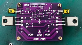
I've finished assembling my amplifier circuit.
I cannot reduce the offset voltage below 3.3v. The sound is fine. Although the offset voltage is 3.3v, the speaker protection circuit does not cut. I'm waiting for your help where I'm wrong.
- Output mosfets 2sj160-2sk1056
- Supply voltage +-18vdc
- Quiescent current 0,75Amp
Check all currents and voltage shown in the schematic in post 1 or latest.
3.3V is too much DC for speakers!
chris
BTW...what is the latest schematic? ;-)

Check for continuity between the MOSFETs metal tab and the heatsink. I had a tiny whisker of aluminium shorting mine out.
Take some voltage measurements around the circuit and compare with the schematic. Post your findings of there is anything abnormal.
I assume that you know the trimmer is a multi-turn so you have to keep on turning for a bit to get it to change.
Were your Jfets matched at all? I matched idss on mine to be fairly close to minimise the offset to be trimmed out.
Here is the final schematic I have posted
https://www.diyaudio.com/community/...on-output-10-watt-class-a.389498/post-7446866
It is a nice little power amplifier 🙂
https://www.diyaudio.com/community/...on-output-10-watt-class-a.389498/post-7446866
It is a nice little power amplifier 🙂
Thanks Nikos.Hi my friend .
congrats for your building.
with all respect i think you must raise a little the compensation cap.( these small cracks at vertical line and the litle overshooting in corner ).
Would sort of value do you recommend?
Check for continuity between the MOSFETs metal tab and the heatsink. I had a tiny whisker of aluminium shorting mine out.
Take some voltage measurements around the circuit and compare with the schematic. Post your findings of there is anything abnormal.
I assume that you know the trimmer is a multi-turn so you have to keep on turning for a bit to get it to change.
Were your Jfets matched at all? I matched idss on mine to be fairly close to minimise the offset to be trimmed out.
After connecting the mosfets to the heatsink, I checked to see if they were in contact. The mosfets do not touch the heatsink.
It will make measurements according to the published scheme. When measuring, there should be a signal input. I adjust the quiescent current with R6 and the offset with R7. Jfets are not mapped. I suspect the Jfets. I run it for 15-20 seconds, the sound is fine. I read somewhere that there is a virtual offset in the outputs.
I recommend also raise the compensation caps.Hi my friend .
congrats for your building.
with all respect i think you must raise a little the compensation cap.( these small cracks at vertical line and the litle overshooting in corner ).
Now is 47pF and 220pF
Like this.
I finally managed to run it properly.2sk170s were suspected to be original.I replaced them with 2sk163, which I am sure is original.I made IDSS mapping.offset voltage around 3mv.quiescent current 0,75amp.Thanks to everyone who helped.
Attachments

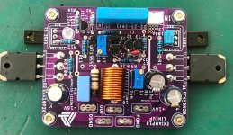
The 2sk170s were unused and checked. But I could not reduce the offset voltage below 3.3vdc. When I installed the 2sk163s, the problem was fixed. After that, it remains to collect and box the second card.
Hi @lineup wouldn't it be a good idea to add a capacitor in series with R4 so that the DC gain goes down to 1, that should further reduce any eventual DC offset due to component imbalances, or what would the reason be to leave out a series capacitor in this position? If we would add an optional capacitor here, what would your simulator think is a suitable value for it?
I am not sure this would help @fazildiken but it may be worth to try out adding a capacitor. Fazildiken, if you switch place for the JFET's in position U1 and U2, does this change the DC offset, for instance would it go in the other direction, ie. becoming negative instead? Have you checked Gate leakage current, just in case if one of them is partially damaged?
I am not sure this would help @fazildiken but it may be worth to try out adding a capacitor. Fazildiken, if you switch place for the JFET's in position U1 and U2, does this change the DC offset, for instance would it go in the other direction, ie. becoming negative instead? Have you checked Gate leakage current, just in case if one of them is partially damaged?
2SK170BL or LSK170BSorry if this was answered already.
Which Idss grade 2SK170?
GR OR BL?
Post #90
https://www.diyaudio.com/community/...on-output-10-watt-class-a.389498/post-7446977
Is where is a PCB file
https://www.diyaudio.com/community/...on-output-10-watt-class-a.389498/post-7446977
Is where is a PCB file
- Home
- Amplifiers
- Solid State
- Scope Design: JFET Input EXICON Output 10 Watt Class A