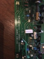
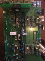
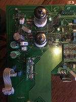
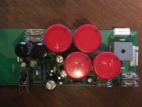
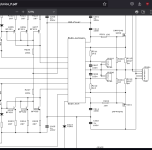
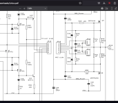
First of all, this is not a beginners amp to repair.
Supply voltage is on the high side, but not excessive.
Max drain voltage on your data sheet is 200 V, not 44.
Voltage will drop as soon as the amp starts to work.
No need to test the devices out of circuit at this moment.
To be sure check also source resistors R 213, R 214.
Bias circuitry receives power via the driver stage, did
you check Vd +/-, F1, F2 ? Check all supply voltages.
Thanks.
Yes i have checked the bias resistors they are good. Both Fets have their supply voltages but bias is zero which i thought was strange but might be how the bias control boards work? As you can see the board is printed corresponding closer to the first schematics you posted Rev C. It does not correspond well to the Unico P schematic.
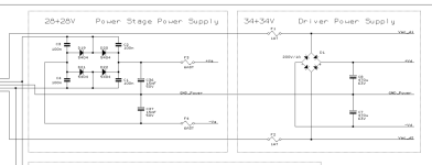
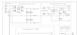
I thought voltage would probably drop under load. But in the Unico P schematic it lists +-33V as the supply voltages and in the Rev C schematic it lists +-34V This is why i thought +-46V is a bit high although i understand it should drop under load.
All of the fuses test good.
The IC's on the bias boards look like they have had the codes erased which i thought strange unless they have suffered.
I just didn't want to go further until i could confirm the correct primary winding config for 230V
Waiting for Unision Research to reply after their first reply which was to contact a distributor. I have asked them to simply confirm the jumper configuration on the mains input board for 230V as it's not in the schematic or printed on the board.
I think the issue is in pre-drive side but i am yet to go through it with the scope. I don't really know enough about the valve part of the circuit to fully understand it.
I am checking other resistors around the final mosfets.
In circuit the 1M are around 700K i think that is ok in circuit.
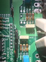
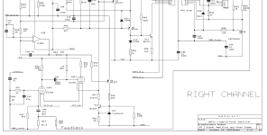
R45 and R46 as they are 2,2K which test fine but in the rev c schematic it shows 100 ohms. They look original, nobody has worked on this before other than the primary transformer input voltage selector as photographed earlier.
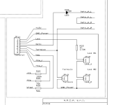
It's easier to refer to rev C schematic for the print on this board but then i have to look at the Unico P schematic for the actual values.
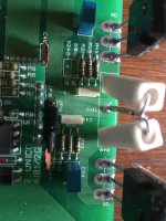
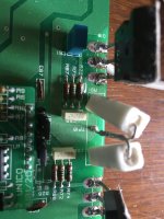
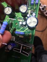
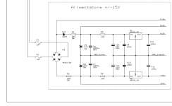
Ok. I found something. R17 on the PSU (large wattage) is open. It is supposed to be 330 ohms! It's jumping around 2.2Kohms!
Attachments
Last edited:
I don't think i have anything suitable in stock will double check. I think it's a 3W bit annoying when the schematics don't fully correspond.
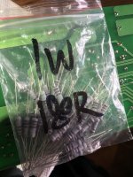
I could probably hash something together with these for testing. I would need 8 just to get 340 ohms at 2 watts.
I'll look in the used pile.
I alsofound some big resistors in an old TV board but i can make 370ohms I think i will just order some. I'll be back!
I could probably hash something together with these for testing. I would need 8 just to get 340 ohms at 2 watts.
I'll look in the used pile.
I alsofound some big resistors in an old TV board but i can make 370ohms I think i will just order some. I'll be back!
Attachments
Last edited:
Nope i got that wrong too. I read it wrong those are 2.2K and testing ok. I made an assumption after testing them in circuit as one was testing 33ohms and the other at over 2k When i saw them next to each other in circuit i assumed they would test the same. I need to take a closer look at the circuit in case on is being pulled low by something else but it's possibly just the circuit.
Back to the drawing board. And no need for the franken resistor i just put together. My brain is not working today. Wasting my time again to help someone out. Getting sidetracked by the psu when voltages seem fairly normal if not a little high on the fets.
Back to the drawing board. And no need for the franken resistor i just put together. My brain is not working today. Wasting my time again to help someone out. Getting sidetracked by the psu when voltages seem fairly normal if not a little high on the fets.
I'm just going to go back to square one and do what i was going to do to start with and follow the signal with my scope. I need a break from this right now.
I still would like to know the primary transformer configurations if Unision Research will tell me but i have a feeling whoever is on the other end of the line has no idea.
It was the lamp filament in the tubes / valves that was lowering the resistance of R21 when i measured it.
Now i found them i can see why they were measuring totally different to each other.
Other curiosities that remain unanswered is does this have a phono stage and is there a way to config between aux and phono and what do the jumpers next to the bias boards do?
The owner said he has swapped the tubes with some others he had to test them and said there was no difference. I assume the others also were in working condition. I'm guessing this has something to do with the opp amps or the pre-drive side but still confused why bias is zero and mosfet voltages are high. Also i dont really understand the purpose of the tubes in this.
Attachments
Last edited:
No idea of your skill level - do not hurry with this one.
Make yourself clear about the model and correct schematic.
It seems you want to confuse us, reading red/red/red
colour code for 2200 as 330 and reading the 180 ohms
resistors as 18 is just a nightmare of repair skills for me.
Also do not confuse yourself caring for the mains wiring :
all this has been working for years in your area with this
setting, right ?
And how is the phono question related to the amp fault,
why even ask? Do not expect a phono input with missing
phono board.
I gave instructions here and with personal communication.
I will be out if you don't follow. No need to check resistors
before you measured all supply voltages.
I confused myself quite a bit the other day. I actually was getting 33 ohms on the meter. I am terrible at memorising color codes and i made a mistake reading it as 330 on the meter but it was actually showing 33 ohms. It was the heater element of the valve that was pulling it down from 2.2k to 33 ohms.
When i saw the two 3W resistors side by side i assumed they were each performing the same task.
I got a little excited and assumed one was open when actually they are both 2.2k and they perform different tasks as i saw later.
We do not know the history of this amplifier. I met the owner recently when i drove 2 hours (in France) to pick up two Quad II monoblocks from him. He has lots of gear laying around in a bit of a mess and i proposed to him a repair service if he needed anything done. Since i drive past his area at least 2 times per year. I offered to do one item at a time. He does not know where it came from but he thinks from the UK. He said he has tried different tubes / valves so we are at least fairly certain they are ok.
I have checked the 5V, the 12V the + and - 15V Until i saw the schematic i thought +- 46V was ok on the fets.
When i take another look i'm going to check more supply voltages. It's a bit confusing reading between the two schematics for now.
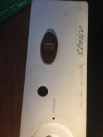
As for the model. As far as i can tell from photos and videos online it is the Unico P The model is not written anywhere except for the numbers i gave from the main board i had no idea of the model until i saw it was a Unico P.
The silk print corresponds to the numbers from the Rev C schematic but the component values correspond to the Unico P schematic.
I am referring between the two different schematics to help me navigate via the Rev C schematic and then find the values on the Unico P schematic.
I was mainly curious about the phono stage because on the rear panel the 1st input from the end is marked Phono / Aux similar to Cambridge audio amplifiers) if they have the phono stage fitted. I was wondering if it needs to be set by changing a resistor position or something. I was asking because perhaps if someone plugged a line in while on phono they may have over driven both channels at the same time.
Yes i may have rushed it a little and i have not had time to really study the signal path yet. I may have assumed the TL052CP opp amps could have been part of the phono stage. I can not see anywhere another board can be fitted. The opp amps have their +-15V.
Without a print of the underside of the board it's a little tricky to follow the signal path so i'm going to spend a bit more time looking at it to try to better understand it.
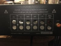
We can see on the rear that it was originally 240V which implies UK but as in the photo i posted earlier we can also see that someone has changed the solder bridge on the AC primary input board.
I still need to check the igh voltage supply to the Anode. I do not know much about testing / troubleshooting valves.
I will check the anode voltage before i do any scope work on the input path. I did not look for a high voltage supply yet. Heaters seem fine as the valves are glowing as one would expect.
I gave up learning resistor codes 40 years ago. I have a terrible memory in general, things such as math procedures and the like escape me, one reason you will probably never catch me learning morse either.
Attachments
Last edited:
Yes. That's the Rev C schematic i've been talking about. But some of the components values i thought corresponded to the Unico P schematic. I'll have to look again. Mostly i've been looking at that one you first posted. Rev C, as you said, post 27.
I'll post back in a few days. I'm overwhelmed with kids right now.
I'll post back in a few days. I'm overwhelmed with kids right now.
I had to pinch myself to check i wasn't going mad. Here is an example of what was confusing me. After checking the bias resistors again the other day i went through some more resistors in the general zone. Check R45 and R46. Installed are 2.2k where Unico Rev C states 1k but Unico P says yes to 2.2k. Perhaps this is the only example and nothing important but this is something that threw me off when i started looking at both schematics. That and not knowing the specific model name.
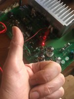
One of these became a little scarred after trying to measure it out of circuit. I detest when people design their vias to fit the exact size of the component legs and on-top of that they do a fine job of bending the legs out on the tinned side. I've been meaning to throw the new element in my de-soldering gun for a while but still, what a mission on these tight fitting boards!
One of these became a little scarred after trying to measure it out of circuit. I detest when people design their vias to fit the exact size of the component legs and on-top of that they do a fine job of bending the legs out on the tinned side. I've been meaning to throw the new element in my de-soldering gun for a while but still, what a mission on these tight fitting boards!
Attachments
The only clue i can find right now is the +-24V supply. I started to look at -24V as i only have +-20V on R1 and R2 When i lift the leg of R2 I get -30V rather than the -20V i am getting with it in circuit. Could something around here Q6 Q12 D17 be pulling -24V down to -20V? Nothing seems warm.
I'm still trying to get my head around how the input signal path works between the valves and the opp amps.
With the valves removed i get 1 Volt closer to +-24V and loose audio. I also get a red led on the Atmega controller board.
So i'm not sure if it's supposed to be 24V or 20V as some parts are different on this board. Another example of this is R211 on ground power in is 47Ohm 5W and not a 10Ohm 3W as in the schematic.
Lifting R2 also takes out my -15V supply which seems fine.
R1 and R2 are quite warm (no difference with valves removed), enough that i can't leave my finger on them for too long. This suggests that something is drawing a fair amount of power, obviously being 3W i think they are designed to take a bit of heat being voltage droppers. So i'm not sure now if something is pulling the +-24V supply low or if it's actually supposed to be +-20V.
I checked anode voltage and i'm fairly sure i've checked all other voltages.
One thing i've noticed is that when i unplug the thermal fuse from the mosfet heatsink is that it makes no difference, sound is always super quiet and a bit distorted.
I'm going to try to trace the audio signal but it's a bit tricky.
Attachments
Last edited:
I could not get more than -22V even after removing D17 Q12 and Q6 and the valves. I suspect I am not supposed to see -24V on this unit.
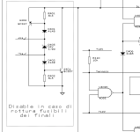
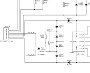
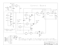
My attention goes back to the thermal cut off. I am going to try to understand better how the nand ic control board works. I have a feeling that the thermal cut off or other cut off is enabled or possibly there is an issue in this nand control board. With the thermal fuse connected it connects pin 5 of this control board to ground. After that i'm not sure exactly how it disables the amp but i suspect it has something to do with disabling the bias boards. The board shows an opto connection and i can only think this must to be something to do with not getting power to the opto isolators on the bias board or perhaps cutting power to the bias boards. As mentioned previously Bias is zero which i find strange and i could not measure much voltage present on the bias boards. D22 is a red LED on pin 4 of the nand that is from the opto output after D22 it goes to pin 4 on the Right channel bias board. the thermal switch is on pin 5 of the nand and for the opto isolator to work it needs Vc_k_R or (L) depending on how you intepret the misprint on the schematic.
The schematic of the nand control board mentions to disable or perhaps that it will disable in case of a broken "final" fuse. I'm wondering if it means the thermal fuse and is there a way i can disable this protection.
The schematic has it's rights and lefts mixed up on the pages with left and right channel.
I need to find Vc_k_R or (L) / opto_K_R coming into pin 5 on the bias board.
D22 never lights weather the thermal fuse in in or not. I assume D22 is supposed to light during normal function indicating no signal from the nand board.
Next i will search Opto_K_R and spend more time looking at the nand control board. I will also check that D22 is good as it could potentially break the path to the bias board opto.
I think isee a little clearer how it works as far as the opto isolators and the bias boards. Opto output from nand passes through D22 then to the 1st R opto isolator then out of the opto isolator and into the opto isolator on the L bias board then out of here back to the thermal fuse and to ground. I need to find out why opto is not present from the nand board.
I'll be doing some testing later including testing some voltages and smd transistors on the nand board where Q404 seems to test ok, i will now check for 12V on Q404.
I've only got 5.7V on the nand board vcc 12V line. Now i'll try to find out why.
Attachments
Last edited:
I put the valves back in because that was triggering the red led on the atmega board. Now i have 11V. Not 12V that i remembered from 1st testing. But i have some components removed still so perhaps this is why. I'm going to refit the components back on the board and check D22 and the return to ground via the opto isolators as now i have 11V on Q404 output, it should be enough to drive the 2 optos and D22 if there was a return to ground.
I need to check some more voltages on the bias boards once i get the other parts back in because i'm currently seeing 7V on Rch Bias board pin 3 but only -0.69 on pin 3 of Lch bias board.
Going into D22 i have 11V but after D22 i only have 1.8V. The final opto does return to ground so i'm thinking one led or opto might be blown.
A quick update. D22 was blown, i have fitted a larger red LED as i only have the smaller type in UV which i think are a different voltage. I hope having a 5mm LED is not going to take too much power from the optos. Now D22 lights after the initial 30sec timer is completed. After replacing Q5 i now have +0.69V on pin 3 of the right ch bias board. Either this is correct or Q5 and Q14 may have issues. Not sure. I'm about to replace Q12 Q17 and D6 and give it a test to see if D22 was the culptit.
Well 16 hours work to understand these often confusing schematics just to realise an LED was blown taking out the entire amp!
I hope this post saves someone some time and money. CHECK D22!!!!
This is a great project for beginners!
Thanks to as_audio for supplying the schematics and other info.
I hope this post saves someone some time and money. CHECK D22!!!!
This is a great project for beginners!
Thanks to as_audio for supplying the schematics and other info.
Attachments
Last edited:
The wild goose chase for +-24V cost me some time! Only having 20V is probably due to this amp being configured for 240V while i'm on 230V. I've just checked my emails and more good news. Unison research..... The input board settings for different AC voltages!
Attachments
Last edited:
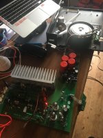
Turns out the last attachment has the input voltage settings for the Unico P model. If i manage to get the Primary input voltage settings for the Unison Unico Rev-C i will post them here. I forgot to mention that water had been leaking onto this amp at some stage but it was obvious that this had never been while power was applied. My guess is that one of the previous owners more or less discarded it once it became broken and at one point it was stored badly. I spent quite a bit of time inspecting and cleaning it up before i made a real start on trying to figure this thing out. Today i put everything back together. I sanded and painted the inside of the chassis where one corner had rusted. My tip is to use a can of black stone chip paint (well shaken). The texture seems to resemble the plastic coating or whatever paint they used, after sanding i applied 3 light coats in the area and it looks great. The owner will be happy to get this back and to finally be able to enjoy it.
- Home
- Amplifiers
- Solid State
- Schematic diagram of Unison Research Unico
