Super work Rahul!
The RMIE version will be a helpful option
Your timing is impeccable, just about the 3 year SCG anniversary.

The RMIE version will be a helpful option
Your timing is impeccable, just about the 3 year SCG anniversary.

The middle one is sized to go over the original board, so you can borrow power from the original board and then use the new circuit.
Like most decisions in my life, I plan to take the middle path.
You are much too kind Rahul. If anything I have felt I was selfish to take so much from you without any return. You have taught me much. Your patience sets an example for me to follow. As you can tell from my "exchange" I have work to do on that. I am overly protective of those dear to me as though you need my protection!
I cannot wait to rebuild my "stages" with proper PCBs.
Now that I have made my first purchase from JLCPCB I am ready to proceed when you are ready.
I cannot wait to rebuild my "stages" with proper PCBs.
Now that I have made my first purchase from JLCPCB I am ready to proceed when you are ready.
So you are retaining the stopper for Q103?
I finally removed the 2SJ74 I had in the tweeter amplifier line stage with J175 and can fully agree with you. It does sound better - much more relaxed. Makes no sense that this esteemed part doesn't sound as good as the peasant's choice but then I have always had a preference for the company of peasants over the esteemed.
When I did this I removed the stopper from J175 and increased the capacitance in the power supply from 0.1 to 4uF. Could 0.1 uF be too little? I did like it better than the 100uF electrolytic but I think the supply is quieter with 4 uF.
You never gave us your reasons for that change - not that you have to though I would be interested to know.
Keep putting off trying out the buffer. Any voltage guidelines? Any pitfalls?
Thanks and take care,
After the regulator, there is usually not a need for more capacitance. I like it better with no or very low capacitance. This is very audible on a DAC supply that feeds a clock. Here 0.1-10 uF probably doesn’t result in audible differences. But give other values a try. On the new boards, I made room for the Wima DC Link caps, both for input and output coupling, and also for a power supply bypass and a localized source of energy. I haven’t tested it yet but seen it in the books. Btw, the Wima DC link caps are amazing.
Indeed. Any regulator behaves in this way, increased output capacitance reduces both undershoot and overshoot magnitude. BUT it also increases the duration of the transient response, and we don't want that. Now, if regulator is close to load, really there is no need for a large output capacitance (unless it is specifically stated by the manufacturer to achieve stability).I like it better with no or very low capacitance.
Three boards, ready to go.
1. The large one is intended to fit into a standard diyaudio chassis and it has onboard provisions for switching two inputs and the volume control.
2. The middle one is sized to go over the original board, so you can borrow power from the original board and then use the new circuit.
3. The last one is for Rick, who has provided me with tremendous support and encouragement throughout the development of this new version. I'm calling it the 'RickMcInnis Edition.' It is actually a really neat idea because this smaller card can be put into the chassis of power amps, such as various follower and other amps, such as the VFET, SIT, F4, and others. Thank you Rick!
What power supply board will be best suited for the big board?
I have one designed and ready to be tested already. Just need to order some caps. This will provide impetus. The circuit was posted earlier. It was the standard zener follower. Improved filtering. Shunt and other options can be used. I’d shoot for 60-70V out.
Hi folks, this last week was very busy at work. I have the RMIE version PCBs and have started populating them. I expect to finish testing this weekend.
Take your time, Raoul! And Happy Holidays to you and your family. I am going to visit family in Minnesota, so no build until January for me!
I was not sure if you were going to make the pcbs or get us to make our own.
If you have them made them I will get them from you. Of course.
If you have them made them I will get them from you. Of course.
After testing, I am putting the gerbers here so you can order your own 🙂
Testing of the RMIE version is complete. It went smoothly. Final version will have a couple of changes to the schematic. Using J175 instead of J176 in the output buffer. Just a bit more headroom and it sounds better. I've gone through so many buffer iterations but really, this is the final now. And the J175 needs a slightly bigger source resistor, at 130 ohms. Also took out a jumper and adjusted the bypass cap value. I just finished editing the PCB. It is ready to go. Hope to post the gerbers, schematic, and BOM tomorrow.
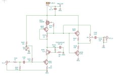
Here it is folks. Schematic, gerbers, and BOM attached.
Few notes:
1. Testing jig schematic is attached to this post. Use that to measure Vp (JFET pinchoff or the voltage at which almost no current flows through the drain and source of the JFET) across the 1Meg resistor and for testing JFETs for other positions.
2. A lot of 10 J111s, 20 J175s, and 20 J113s are needed at a minimum to select JFETs for various positions. Don't worry too much about channel matching. If you get two exact matches, great; if not, no problem. The circuit is immune to small changes in device properties. Bigger lots will give you a higher chance of matching between channels, but this is not strictly necessary.
Note below that J175 and J113 are used twice in the circuit. Each circuit position of the same JFET requires unique selection. Pay close attention to the JFET selection procedure below and put the correct JFET device in the correct position on the PCB after you perform the selection.
J111: Select the two with Vp closest to zero, one for each channel.
Q101 J175: Select the two with Vp farthest from zero, one for each channel.
Q106 J175: Select two out of the batch that measure 10-11 mA at 130 ohms source resistor. Replace the 1Meg resistor in the test jig with 130 ohms and measure the voltage across the 130 ohm resistor. At 10 mA, it would read 1.3V.
Q103 J113: Select two out of the batch that measure 15-20 mA at 10R. Replace the 1Meg resistor in the test jig with 10R and measure across 10R.
Q105 J113: Select two out of the batch that measure 10 mA at 47R. Replace the 1Meg resistor in the test jig with 47R and measure across 47R.
3. Note the orientation of the JFETs on the board. The flat side goes with the flat side of the JFET. The J175 is immune to orientation, i.e., it can go in reverse and still work fine. For the Q101 position, I have a slight preference for J175 going in reverse relative to the PCB orientation. YMMV.
4. Power supply: I suggest anything from 50-70V. Don't go above 70V otherwise you are pushing the dissipation limit of the little guys.
5. Jumper JP1 conveniently provides a way to either use the buffer stage or bypass it. If you are driving an F4, say, which has an input buffer, feel free to skip the output buffer of this preamp. Now, on the other hand, if you want to drive a big MOSFET or SIT directly, like in a MOFO or the TDV, then I'd recommend using the output buffer. On JP1, the pin closer to the JFETs is connected to the non-buffered output.
6. The only setting on the circuit is RV1. Turn the pot to achieve the midpoint of the supply at the output before C102. Most easily measured at the leg of C102 closest to JP1. For example, for a 50V supply, turn RV1 to 25V at the output.
7. As usual, stuff the smallest parts first. Start with resistors, then JFETs, then the caps and other parts.
Hope you have fun!
Attachments

Last edited:
It could but I want to continue testing. I just got some new planar headphones from HiFiman, the cheap ones 🙂Does the headphones buffer remain the same?
- Home
- Amplifiers
- Pass Labs
- Schade Common Gate (SCG) Preamp