Hi
I believe if these particular jfets were reliable for 40V that National Semiconductor would have rated them for it as it would be a selling feature. Even were that so, in a push-pull circuit the devices have to be rated for the full breadth of the supply which is the voltage window the signal lives within.
A 40V peak signal is 80V peak-to-peak. When one device goes off the other turns on and the off device has 80V minimum across it. This is quite in excess of the 25V rating.
Even if you meant 40Vpp, you have 80V across the two devies ar idle - 40+40 according to a previous post. The 40Vpp is 20Vpk, so when one device has 60V across it the other has 20V. Again not a voltage environment I would subject these devices to.
I have seen 25V rated jfets "wear out" in 24V circuits where they are used as gain elements running at low currents (<1mA or so). So, I am not inclined to believe that your luck so far can be considered to be proof. Maybe because of how jfets are constructed they have to have an excessive nominal capability to reliably be rated at a much lower voltage? It would help if we could hear from an engineer who designs jfets.
The attached data sheets indicate 30-35Vds. The Interfet sheet gives a misleading BVgss=55V, which is an insulation rating for the gate with D and S shorted.
In any case, you really must review the data sheets and read the fine print. Anyone running these devices at the voltages you promote will be pretty annoyed when the devices fail. Please also review how devices should be rated for push-pull circuits.
Attachments
Okay, thanks for the info. I do read datasheets and am well aware of the ratings. The peak voltage swings you are talking about are AC; the DC conditions do not change. I do appreciate the warning but I don’t think we are treading new ground with respect to operating the JFETS at or a little above the ratings.
Rick has also built this circuit and can chime in with his experience. Maybe you can share some more info on which circuits the JFETs failed when operating at 25V. Over the past one to two years of working with these devices, I have not had any failures.
Rick has also built this circuit and can chime in with his experience. Maybe you can share some more info on which circuits the JFETs failed when operating at 25V. Over the past one to two years of working with these devices, I have not had any failures.
Hi
No one said the DC conditions change.
You do not seem to understand that your buffer is a push-pull amplifier. The total voltage across the two devices will be impressed across a single device at the extreme signal peak. This is the same in a split-rail power amp, or single-rail amp. The supply sets what the maximum peak-to-peak signal can be and at the output node, each device connected to that node has to be rated for the full pk-pk voltage NOT just one peak, not just for half the supply.
You are not exceeding the 30V lomit of the jfets "by a little bit" - you are wildly exceeding them to more than twice their rating.
I don't think I can make this any more clear, so I will just call it quits here.
Check this design:
https://www.firstwatt.com/wp-content/uploads/2023/12/art_diy-fe-2022.pdf
By your logic, the J113s would not be appropriate for this circuit with 50V supplies. There are many PP examples as well.
If someone is uncomfortable with a higher supply, they can always go lower. This is diy after all and these devices are dirt cheap.
The proof is in the pudding. Maybe I am just lucky but I think not. Don’t assume what someone does or doesn’t know. I don’t need the condescension.
Hi
I have seen Nelson's article and disagree with applying that much voltage to the J113 in the output CCS position. The CCS and the BJT can both see the full breadth of the supply rails over the signal cycle, which means both devices must have a rating higher than the total supply applied - not just for one rail. For the other positions, it is expected to see 23-29V rails from the F4 or similar Unity PA and each J113 only sees one rail. That is within the data sheet spec for the device.
NP is a brilliant guy and I have admired his work for decades, but he is also Human and can make mistakes like everyone else.
ra7: I apologise if I was condescending, but... When you say the two devices are 40V each so stacking them in a push-pull circuit at 80V total supply is okay, I really have to wonder about what can justify such an action? If you did this in a power amp the output devices would blow up as soon as you applied a signal as that woiuld exceed their rating. NP says the J113 can withstand 70V and maybe it can - it is quite dumbfounding if it is true. Why wouldn't any of the manufacturers of this device say so? So, maybe this is a unique cae and you can get away with the "over voltage".

I really have to wonder about what can justify such an action?
Past experience with the device?
A lot of builders here routinely push devices beyond their official limits with good results. I have seen it time and time again with tubes and solid state devices alike.
Would I order 10,000 units for commercial reasons? No.
But it’s DIY and at the end of the day, all responsibility rests with the builder.
Thanks for bringing up what the data sheet says, so that interested builders can make a more informed decision.
The JFET Frontiers Part II article provides a better and more pertinent example. The left circuit is a single ended follower (While cathode follower with feedback) and the right one is a push-pull follower. I have tested similar buffer circuits both in simulation and in a fully built real version. In practice with today's cheap JFETs, I found the left one had too much distortion compared to the right one. We are operating the current design at about 5V above this level, i.e., with 60V supplies (same as a 30V each positive and negative supply) to accommodate the output FET dissipation limits. If you wish, you can reduce that to 50V to give peace of mind. In the article I linked above, Nelson also mentions that the J113 can sustain up to 70V. I have observed the same in practice. We are well below 70V peak to peak swing.

We may be getting off topic here but I see it as an AC/DC question. Look at the 300B datasheet:
https://frank.pocnet.net/sheets/084/3/300B.pdf
Max plate voltage: 400V and it is often operated at 400V (grid bias) albeit with a transformer. The plate swings symmetrically about the bias point, which means the AC swing goes above the max rated DC voltage when the plate swings up. This is really fine and the curves show that it remains linear above 400V for ac swings, though it should not be biased there.
The J113 spec sheet does not even have a max Vds spec. It has max Vgs and Vgd specs. Also, the devices are rated at 35V Vgd and Vgs. The curves may or may not be linear above 35V Vds, the specs don’t show that. But that doesn’t mean they won’t operate there for AC swing. That’s my understanding. Either way, I am not pushing them beyond 30 V Vds as the bias point. How it sounds there is the real question.
Who would have ever thought that THIS thread in THIS forum would be infected by DIYAudio Protectors of the Known Audio Universe syndrome?
Those creatures who rarely build anything but know their way around SIM CITY. Spend more time time making posts than listening to music.
Who knows if the moniker is a joke or a confession but asking a question is fine - then wanting to start an argument with someone who has made numerous iterations of a circuit and listened to it for countless hours is something that happens in the other DIYAudio forums too often and usually has not invaded this sacred space of PASS LABS.
Oh, well. Any problems I have had with the circuit have been my fault - not the devices. And the devices cost nearly nothing. If mine blew every six months I would not care. But they do not.
Rahul's circuit is simple to build but does require some care and thinking in its implementation. Not that I am an expert builder on the level of Rahul but the circuit has served me well for over a year in various configurations Rahul has given me to try. I have learned LOTS from this interaction with a generous man with two fine ears who builds his gear to enjoy listening to music; circuits that have allowed him to hear more of the music.
If one has doubts about a circuit then don't build it. Your motivation escapes me other than what I assume as I wrote above.
Please take your concerns to another thread or start your own but, in my most unhumble opinion, you will need to do something far more impressive than what you have shown us so far to be taken seriously.
I wish to build this beautiful circuit someday! I patiently await the gerbers....then...lots of noob questions headed this way 😉
A Monk spoke to me about how wonderful it sounds so I must experience this enlightenment.
A Monk spoke to me about how wonderful it sounds so I must experience this enlightenment.
Hi
I looked in my National Semiconductor Fet data book and nowhere does it list "Vds" other than to define it as drain-source voltage, but no data sheet or process data lists a limit.
I looked in my Japanese Fet data book which has a column labelled "V" separate from "Vgs". Strangely, they list a value in one column or the other but not both, for each device.
I checked wiki and other places and only found one fleeting reference to Vds being limited by heating.
One would think the manufacturer would know the Vds voltage maximum since they have to create the wafers?
I can see why you might add Vgs and Vgd to assume a Vds rating, but in all of the curves and data sheet lines the test conditions always use a Vds lower than Vgs max. Nelson's stress test shows that that might be the arc point - a real maximum.
The preamp I referred to earlier is a design Randall used in a line of guitar amps. The supply voltage is 24V and the jfets are used in standard common-source gain stages, so all the currents are limited by resistors.Yet they would age and gain would fall and the fix was simply to put in fresh new ones. The jfets were probably 2N 5485, which I always took as 24V devices. They would never see that much voltage in Randall's circuit.
All of the above lead me to believe that Vds was rated the same as Vgs.
By the way, the two followers you show above are both push-pull. Self has a BJT version in his Small Signal book.
And also, with tube plate voltage ratings it was assumed that the tube would have a reactive load, and most early tube circuits did. So, the Va rating takes into account the flyback voltage of the transformer, while keeping the peak within the arc voltage of the plate. Few data sheets list this. An example that does is the EL-34, rated at 800Va with an arc voltage of 2kV. The lowly 12AX7 is rated at 300V with an arc over above 540V.
Rick: You have no idea what my building experience is and your assumptions merely show that you have too much time on your hands. I don't have time to post here about everything I have built or am building. My spice experience is super limited, being only what I have learned from Bob Cordell's book, and most things I know have been from hands-on methods.
Let’s not escalate any dispute.
Thank you.
In the absolute, what data sheets say matters a lot. But, here, where we try things no one should do at home, it’s all a matter of curiosity and empirical exploration.
onsemi give some limits for steady-state scenarios and says to contact them for pulsed applications. So, their data sheet is not as complete as I would like.
Hi
Most data sheets have a disclaimer that using the device at an absolute limit will deteriorate the device and shorten its life. I noticed this on everything fet-based, including mosfets and solid-state relays using mosfets. Mosfets seem like fragile beasts when it comes to heat and they need as much cooling as you can provide.
Since the Schade Preamp needs low capacitance devices, the following point likely is not relevant: Many larger mosfets have huge gate capacitance and might be an option for a schade power buffer referred to earlier in this thread. Those >300W mosfets need liquid cooling if you want to use their rated capacity. They often do not have a DC line (sometimes given as 100ms) as they are designed for switching circuits, giant inverters, etc.
I did a sim with the small jfets running from 24V. I found the gain to be about 7x with the 1k/10k. Changing to 10k/100k reduced the gain and THD was higher. Where is the original Schade description? Does making the Schade resistor ratio only change the gain, or does it make it behave like a lower-mu triode, or does it simply allow the pentode-like curves to rotate back towards their original shape? half-way would seem sort of "ultralinear-like" maybe 🙂
Adjusting the bottom jfet gate voltage up so the output node was over 12V, more like 15V, gave slightly less THD but limited the swing for the positive signal half to 8Vpk.
Mosfet noise is higher than jfet noise from what I have read, so if you were to try a high-voltage hybrid circuit with a p-jfet in, and an n-mosfet above, does the mosfet effect the noise since it is the gain element? Another thing that is interesting is that jfets designed for switching applications, like the J105, have much lower gate noise than the usual "audio" jfets.
Don't give up on it. These things happen, it seems, to every thread here. They eventually go away and find another place to enlighten.
Rahul is worth following.
Rahul is worth following.
Yeah, @CWelsh52 , interesting things are coming. I am finished with the PCB. Working to check it and then place the order.
Hi
Does making the Schade resistor ratio only change the gain, or does it make it behave like a lower-mu triode, or does it simply allow the pentode-like curves to rotate back towards their original shape? half-way would seem sort of "ultralinear-like" maybe? I found the distortion rose quite a bit when I lowered the Schade value.
The jfet circuit sounds nice with simple music. The only depletion mosfets I have are LN150, so I might try those and see if the higher-voltage circuit has lower THD. As you said, the CS load is cleaner.
I would suggest you add a bleeder resistor across the main filter in the PSU; provides a quicker discharge and then quicker to change things in the circuit before you forget what it sounds like - hehe.
Bleeder resistor. Golly gee, we had never heard of those before. You might find it is quite easy to bleed the supply with a resistor that is not permanently attached before the raw supply is attached to the circuit. The supply bleeds down very quickly when connected to the rest of the circuit. There is no need for a permanent bleeder. Rahul was trying to make the circuit as efficient as possible and found no need for the extra current to be wasted.
Try all devices and report back your findings. Building a circuit would be a good place to begin and then to listen to it.
I suspect you will eventually come around to what Rahul has discovered over his two years of working on this circuit.
You might find that the circuit as prescribed does quite well with big music as well as small. This is not a girl and guitar stage.
It is always a good idea, for those who would like to establish credibility, to try the circuit before making recommendations.
If you read the thread you would have found that Rahul has considered the device you want to try and found it was not what he was looking for.
It very well might suit your purposes.
The circuit has been optimized for what I want it to do: swing 40V comfortably and sound good. It could serve in many different ways. I have a few iterations myself, some using LND150. For now, the focus from me is on doing the PCBs for this version.
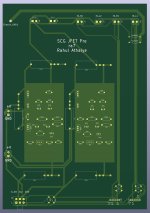
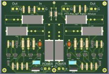
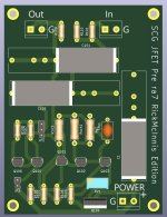
Three boards, ready to go.
1. The large one is intended to fit into a standard diyaudio chassis and it has onboard provisions for switching two inputs and the volume control.
2. The middle one is sized to go over the original board, so you can borrow power from the original board and then use the new circuit.
3. The last one is for Rick, who has provided me with tremendous support and encouragement throughout the development of this new version. I'm calling it the 'RickMcInnis Edition.' It is actually a really neat idea because this smaller card can be put into the chassis of power amps, such as various follower and other amps, such as the VFET, SIT, F4, and others. Thank you Rick!
Attachments
- Home
- Amplifiers
- Pass Labs
- Schade Common Gate (SCG) Preamp