Mr.Metal Sir,, You could use the B+ supply into lm317 ic select correct res value for regulation and whoaaaa no ne4ed for another transfromer. This could power the protection circuit. Evette
Mr. Joseph, Sir,
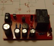
METAL and I designed and layouted a speaker-protection PCB a long time ago (see attatched images).
This PCB proved to be satisfactory by many German DIYers ever since.
It uses of course the Backend PSU AC voltages to power the circuit (as you recommended).
The LSProt-PCB includes a power-on delay, switches the speaker off immediately at power off and protects
the speaker against an AMP's malfunction or DC.
I wonder if we will put the LSProt-circuit on the AMP's PCB.
Best regards - Rudi
Attachments

1K @ 39V: this means that the frontend needs about 40mA current!
No, frontend consume 34mA...(13.5+4mA for differential and led bias + 2*8,25mA=16,5mA for VAS)
Guys,
The math are very simple 🙂
1. For the positive rail: 2x8.25mA for the two current sources + 5mA for the bias LEDs = 21.5mA
2. For the negative rail: 13.5mA for the LTP current source + 4mA for the bias LEDs + 2x2mA for the VAS = 21.5mA
Clear? 😀
Mihai
The math are very simple 🙂
1. For the positive rail: 2x8.25mA for the two current sources + 5mA for the bias LEDs = 21.5mA
2. For the negative rail: 13.5mA for the LTP current source + 4mA for the bias LEDs + 2x2mA for the VAS = 21.5mA
Clear? 😀
Mihai
Good morning Mr.Rudi and Mr.Metal,,Rudi thank you for the gift you sent me,,Also Mr. Rudi remember I also have the LS protect boards and they all work perfectly. Evette
whale pcb
Rudi
This big pcb will not use the heathsink verry efficiently. Can you design it to allow for the front-end psu section to be sepparated?
Rudi
This big pcb will not use the heathsink verry efficiently. Can you design it to allow for the front-end psu section to be sepparated?
Last edited:
Look again more closely at Rudi`s pic in post #157 and you will notice that the front-end PSU is not part of the amp`s PCB and that they`re already seperated.Rudi
This big pcb will not use the heathsink verry efficiently. Can you design it to allow for the front-end psu section to be sepparated?
Guys,
The math are very simple 🙂
1. For the positive rail: 2x8.25mA for the two current sources + 5mA for the bias LEDs = 21.5mA
2. For the negative rail: 13.5mA for the LTP current source + 4mA for the bias LEDs + 2x2mA for the VAS = 21.5mA
Clear? 😀
Mihai
Aye, aye, Sir!
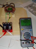
So I built a 1K8 resistor (resulting in a current of 21mA @ 39 V) and measured again.
Stable (after some time) at nearly 41V.
Mihai: is was impossible to order a transformer with 2 x 34 VAC secondaries for the shunt.
I am using a 2 x 35 VAC transformer.
Is this the reason why?
I will have a look at your shunt's schematics and try to lower the output by approx. 2V.
Best regards - Rudi
Attachments
2x35V transformers should not cause any trouble. In Germany mains voltage may vary between +15% and -5% of its rated value and with 2x34V transformers the limits will be 39,1 and 32,3V.
The Zener diodes also have some tolerances.
BTW, what will cost the PCB's and the thermal trak transistors? I need four kits.
The Zener diodes also have some tolerances.
BTW, what will cost the PCB's and the thermal trak transistors? I need four kits.
Last edited:
Mihai: is was impossible to order a transformer with 2 x 34 VAC secondaries for the shunt.
I am using a 2 x 35 VAC transformer.
Is this the reason why?
I will have a look at your shunt's schematics and try to lower the output by approx. 2V.
Best regards - Rudi
The output voltage is regulated by the zener diode ... maybe your diode is not what should be ... 😉
Shunt PSU is very simple. It consists from two elements, a current source (CCS) which deliver constant current on a constant voltage source who in turn regulate the output of PSU's. The current through internal PSU's voltage source subtracts from the CCS minus delivered current to supplied circuit.
In my design the PSUs CCS deliver around 42mA current, half from this current is delivered to the input stage of the amplifier and the other half to the internal constant voltage source.
Hope this is enough for you in order to understand the working principle.
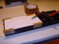
I did some small progress with the AMP tonight, continued with soldering the frontend and drilled the prototype-heatsink.
The shown heatsink will not be the one that I will finally use.
I need to get familiar how to tap (?) a heatsink. That is why I use this one.
I will try and solder the "underneath-transistors" tomorrow.
Mihai apologized for causing my confusion about the output of his shunt regulator.
He simply wrote down a wrong value for the ZENER diode in the BoM.
The ZENER should be a 37V type.
Mihai told me that my shunt (generating about 40.5V) will work without problems with his AMP as well, and I will therefore prototype
the FC-100 with the shunt I built.
But I will keep in mind to change the BoM to include a 37V type ZENER.
Best regards - Rudi_Ratlos
Attachments
Mihai apologized for causing my confusion about the output of his shunt regulator.
He simply wrote down a wrong value for the ZENER diode in the BoM.
The ZENER should be a 37V type.
Mihai told me that my shunt (generating about 40.5V) will work without problems with his AMP as well, and I will therefore prototype
the FC-100 with the shunt I built.
But I will keep in mind to change the BoM to include a 37V type ZENER.
Best regards - Rudi_Ratlos
http://www.diyaudio.com/forums/solid-state/111756-rmi-fc100-single-stage-audio-power-amplifier-7.html#post1413151
post 249
Guys,
Doesn't mater to much if the shunt is putting out 1-2V over the published 39V.
So, you can use any 37, 38, 39V zener diode ...
Kind regards,
Mihai
Doesn't mater to much if the shunt is putting out 1-2V over the published 39V.
So, you can use any 37, 38, 39V zener diode ...
Kind regards,
Mihai
PCB possibilities?
Any news on the pcb's?
I put my name on the wish list.
I'd like to know if the boards are available.
It seems the list no more available. It askes password to enter.
from Metal post 143:
You can actually put your name here:
https://docs.google.com/spreadsheet/...xVUQ2clE#gid=0
regards
Any news on the pcb's?
I put my name on the wish list.
I'd like to know if the boards are available.
It seems the list no more available. It askes password to enter.
from Metal post 143:
You can actually put your name here:
https://docs.google.com/spreadsheet/...xVUQ2clE#gid=0
regards
Yes, that's true. Rudi and I decided that we will make this list unavailable until Rudi finishes his prototype assembly and listen to the amplifier with our PCB.
After we have a running prototype of this amplifier, I will re-open this list for public. As Rudi has already succeeded with the shunts regulator for the front-end I am working now on the PCBs.
regards
Omar
After we have a running prototype of this amplifier, I will re-open this list for public. As Rudi has already succeeded with the shunts regulator for the front-end I am working now on the PCBs.
regards
Omar
Hi ZSAudio,
I have a job and have to work hard for my income; so I do not always have the time to DIY.
I took a day off today and made some nice progress.
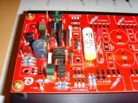
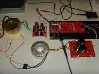
I finished the front-end yesterday night and powered the AMP on for the first time today.
Everything "works as designed"! 😀
No broken fuse, no smoke, all 5 LEDs are burning, I even see the "500 Hz sinus" that I fed to the input and measured
on the MJE15035 driver's collector on my oscilloscope.
Until now I have only had one (mechanical) issue.
The position of the MJE drivers on the heatsink is too far outside, and since I am currently using 10mm spacers,
their legs could not reach the PCB.
I will correct this on the new layout and drill-master.
I will go on now and solder the backend PSU and the output-transistors, ...
I am quite sure to get this done during the weekend.
I will keep you updated.
Best regards - Rudi_Ratlos
I have a job and have to work hard for my income; so I do not always have the time to DIY.
I took a day off today and made some nice progress.
I finished the front-end yesterday night and powered the AMP on for the first time today.
Everything "works as designed"! 😀
No broken fuse, no smoke, all 5 LEDs are burning, I even see the "500 Hz sinus" that I fed to the input and measured
on the MJE15035 driver's collector on my oscilloscope.
Until now I have only had one (mechanical) issue.
The position of the MJE drivers on the heatsink is too far outside, and since I am currently using 10mm spacers,
their legs could not reach the PCB.
I will correct this on the new layout and drill-master.
I will go on now and solder the backend PSU and the output-transistors, ...
I am quite sure to get this done during the weekend.
I will keep you updated.
Best regards - Rudi_Ratlos
Attachments

Last edited:
Hello gents,
that's a good news that there's is a progress in the project. You're correct to test the boards well before offer it to the public.
From Rudi:
"I have a job and have to work hard for my income; so I do not always have the time to DIY."
I know this i sometimes have the same issue. Sorry if i seemed to be pushing you guys but i do'nt want.
I'm eager to get those beauties.
Thanks for your great efforts to share your works with us.
Best Regards,
zsaudio
@ZSAudio,
I made an extra solder-shift especially for you.
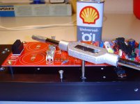
I am now done with the prototype of this AMP!
Tapping the heatsink was not a problem at all.
I found a nice video in YouTube and did it exactly as it has been described there. 😀
But I found another (mechanical) issue.
@ DIYers of the prototype-round:
The solder-pads of the emitter-resistors are very, very small and the isolation ring around them is very small as well.
Be very careful, when you solder the emitter resistors and measure with a DMM the resistances to the rail-voltages and GND.
An "error" like this happens, when you do the layout on a 25-inch flatscreen and zooming the layout by means of the layout software.
The solder pads and the isolation area around them looked sufficiently big in this mode. 😱
I will of course change the sizes in the layout of the forthcoming group-buy PCB.
I will check the PCB tomorrow again and will then switch power-on.
I keep you informed.
Best regards - Rudi_Ratlos
I made an extra solder-shift especially for you.
I am now done with the prototype of this AMP!
Tapping the heatsink was not a problem at all.
I found a nice video in YouTube and did it exactly as it has been described there. 😀
But I found another (mechanical) issue.
@ DIYers of the prototype-round:
The solder-pads of the emitter-resistors are very, very small and the isolation ring around them is very small as well.
Be very careful, when you solder the emitter resistors and measure with a DMM the resistances to the rail-voltages and GND.
An "error" like this happens, when you do the layout on a 25-inch flatscreen and zooming the layout by means of the layout software.
The solder pads and the isolation area around them looked sufficiently big in this mode. 😱
I will of course change the sizes in the layout of the forthcoming group-buy PCB.
I will check the PCB tomorrow again and will then switch power-on.
I keep you informed.
Best regards - Rudi_Ratlos
Attachments
- Status
- Not open for further replies.
- Home
- Amplifiers
- Solid State
- Roender's FC-100 prototype and builder's thread