Hello DIYers
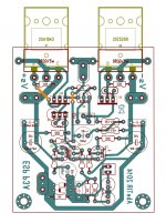
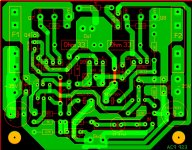
Here is Alex mm sir P3A PCB from post #90, with some correction such as D1 polarity, Some capacitors polarity, Q9 is BC 546, not BD139.as per Orignal schematics of Rod Elliott sir.Is R15 & C7 Connection is right, I think C7 is connected op through r15.Please look and give any suggestion.
Thanks
hi,
kindly refrain from posting same questions in similar threads. it does not help.
DIYA site is a precious resource which is made available free of cost to all of us, like water given by nature..
so lets use it frugally.
Hi Gareth,why you don't draw a general purpose protection board using exactly what you have used in some of your amplifier?It makes for a fun hobby doesn't it 🙂
If you have valuable speakers you might want to add a dc speaker protection circuit next. You can get them on eBay or build your own. It would be a nice little project to build your own - I favour the approach that uses two N-type MOSFETs to make a solid state relay, controlled by a optovoltaic device. There are a few designs around that use that approach, or use regular relays.
abetir,
would you post pcb pdf for your build from post 300 (together with dimensions)?
Hello Ivan,
So sorry, I missed your post. I have now updated my desktop system. I am not so sure if I still had the back up of the lay-out, if you still wanted the pdf files, you could try sending a pm to member Nikosokey. He made a successful built with it.
Sa muli,
Albert
hi,
kindly refrain from posting same questions in similar threads. it does not help.
DIYA site is a precious resource which is made available free of cost to all of us, like water given by nature.
so let's use it frugally.
Hello Prasi
I don't want to disturb any DIYaudio thread values, just trying to ask help sorry for bothering anyone, Did you make P3A Amp using this PCB, or make any changes as I trying to make.please help
Hello Prasi
I don't want to disturb any DIYaudio thread values, just trying to ask help sorry for bothering anyone, Did you make P3A Amp using this PCB, or make any changes as I trying to make.please help
Like I answered in other thread, check out the superR layout that was fine tuned by AndrewT and others and SuperR has measured it also.
http://www.diyaudio.com/forums/solid-state/212342-esp-p3a-layout.html#post3016279
Hey Prasi, I'm sure it's been fixed by now but I noticed a missing trace on your pcb layout. I circled it in red. Ok, just noticed that red wasn't the best color. It's the BD transistor.
Attachments
Last edited:
Hey Prasi, I'm sure it's been fixed by now but I noticed a missing trace on your pcb layout. I circled it in red.
Hey man, that beautiful layout is from Abetir (De Ocampo).😉
regards
Prasi
Last edited:
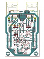

Sorry, my bad. I like the layout though.
Ripcord,
I think you got an older lay out, attached was the correct pdf built by me and Nikosokey.
Albert
(strange I can't advance to page #36)
Attachments
Ripcord,
I think you got an older lay out, attached was the correct pdf built by me and Nikosokey.
Albert
(strange I can't advance to page #36)
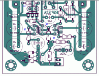
Hello Albert,
Nice layout. One/two suggestions if I may.
1. You could move Q4 a little upwards towards Q5. One would then be able to mount all Q4, Q5, Q9, Q6 on a single piece of aluminium plate.
2. emitter resistors could be moved little towards the center so that there is not even a remote possibility that soldered resistor leads (not cut properly) do not short the base on 5200 or emitter on 1943. looking again, may be this is not that important.
ofcourse these are just mechanical related suggestions.
regards
Prasi

Hello
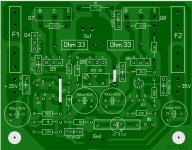
Here is I made some minor changes on Alexmm P3A PCB.Corrected led polarity.Please have a look and correct me if any mistake.
Sorry Input was short, Attach below is corrected.
Attachments
Ripcord,
I think you got an older lay out, attached was the correct pdf built by me and Nikosokey.
Albert
(strange I can't advance to page #36)
Have you heard about "ground loop" problems?
You have one big ground loop on your layouts.
Even if the board seams to work ok, still break it, because it's just looks bad.
I am not sure why have you go all the way down in front of the input with that ground trace, you do not need it, from the 22k resistor on the right, to the 10 Ohm resistor on the left, you can eliminate the entire ground trace, and thus, eliminate the ground loop, and also it would look better.
Last edited:
from the 22k resistor on the right, to the 10 Ohm resistor on the left, you can eliminate the entire ground trace, and thus, eliminate the ground loop, and also it would look better.
like this?
Attachments
- Home
- Amplifiers
- Solid State
- Rod Elliot P3A Layout - Critics