The rev 1.2a can be configed as mc with 56db gain and mm by left some capacitor out, right? I'll take a pair please.
That was the intention originally, but the gain with the caps removed will be only give 29-30 dB, not really enough. So 1.2a is only suited for a mc stage. (You could partially bypass R3,R9 using two resistors in some crazy vertical tent component placement, but I'd rather we didn't go there.)
The switchable 35/56 dB boards are the next out of the oven, 1.3c.
Either way, pm me if interested.
I would like an set of rev1.2 boards for mm operation along with the matched jfets. I live in India , so how do I go about this, ie, how do I pay and what will be the total bill?
Thanks.
Sent from my AO5510 using Tapatalk
Thanks.
Sent from my AO5510 using Tapatalk
Phono boards
The rev1.2 boards only does moving coil cartridges?
I have a MM cart so I need the 1.3 boards right?
You'll need the 1.3c boards for that. Please wait a little until those boards arrive.
The rev1.2 boards only does moving coil cartridges?
I have a MM cart so I need the 1.3 boards right?
Understood!
Ok. Then I will wait for your response when the boards are ready.
PS : What time are we looking at?
Exactly, that's correct.
Ok. Then I will wait for your response when the boards are ready.
PS : What time are we looking at?
just wondering is there a way to improve the com/ground for the crystal P jfet, in Hong Kong the ground is pretty noisy.
I like how the phonoclone3 layout where you have a positive and negative rail and a definite signal and power ground
I like how the phonoclone3 layout where you have a positive and negative rail and a definite signal and power ground
Use a ground lift resistor to isolate signal and power grounds
Sent from my AO5510 using Tapatalk
Sent from my AO5510 using Tapatalk
@sagitis
The CrystalFET doesn't have a negative rail, it's true, but that's just the nature of it.
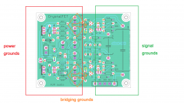
The grounding layout is actually the same in concept as the Phonoclone boards. All the signal grounds are well "in front of" the power supply, and the GND which connects to the chassis and turntable is clean i.e. tied directly to the input return. COM is the dirty return to the power supply.
It may not at first glance seem like the signal and power grounds are separate like in the Phonoclone, but they are so. Since the components are physically separate on the board I didn't have to partition the ground plane in the CrystalFET, the distinction arises naturally from the placement of the components and their connections to the ground plane.
I think the CrystalFET has overall the better ground layout in practice. There are ground planes covering both the top and bottom of the board, and the signal traces are now physically much further away from the V+ rail, with plenty of metal.
The CrystalFET doesn't have a negative rail, it's true, but that's just the nature of it.
The grounding layout is actually the same in concept as the Phonoclone boards. All the signal grounds are well "in front of" the power supply, and the GND which connects to the chassis and turntable is clean i.e. tied directly to the input return. COM is the dirty return to the power supply.
It may not at first glance seem like the signal and power grounds are separate like in the Phonoclone, but they are so. Since the components are physically separate on the board I didn't have to partition the ground plane in the CrystalFET, the distinction arises naturally from the placement of the components and their connections to the ground plane.
I think the CrystalFET has overall the better ground layout in practice. There are ground planes covering both the top and bottom of the board, and the signal traces are now physically much further away from the V+ rail, with plenty of metal.
Attachments
Last edited:
Nice. But will adding a lift resistor do any benefit or opposite?
Sent from my AO5510 using Tapatalk
Sent from my AO5510 using Tapatalk
These things always depend on external variables. It's hard to say.
Generally speaking I am opposed to connecting the signal ground directly to earth anywhere outside the power amplifier. That's why I like external power supplies for the preamp, as that naturally breaks the earth from the circuit ground.
However, for most people it won't be a problem. If it is, you'd have to put 47 ohms or whatever between GND and chassis. That would probably sort it out. Or use a 2 wire power cord.
Last edited:
I was thinking of putting the resistor between signal gnd and power gnd. Or am I worrying unnecessarily
Sent from my AO5510 using Tapatalk
Sent from my AO5510 using Tapatalk
(anyone else feel free to jump in here...)
The lifts I've encountered have all been between the circuit common and an (earthed) chassis. On the assumption of a potential difference between the phono stage ground and the preamp ground generating unwanted noise, adding resistance to the signal ground as you are suggesting will amplify the noise voltage, not reduce it.
The lifts I've encountered have all been between the circuit common and an (earthed) chassis. On the assumption of a potential difference between the phono stage ground and the preamp ground generating unwanted noise, adding resistance to the signal ground as you are suggesting will amplify the noise voltage, not reduce it.
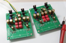
Partially completed rev 1.2a crystalFET tested.
1. Boards are good.
2. Power supply voltages, currents as simulated.
3. Amplifier stage LTSpice values conform exactly to the measured DC voltages when the measured JFET I_dss and V_gs0 values are used in the model.
4. Confirm no need for heatsinks.
So, not only are the boards and simulation working, the procedure used to match and grade the jfets is also working.
Yay!
Attachments
rev 1.2a board arrived today.
They are green. And they are not rev. 1.3c which will arrive later this week. And they'll only work as an mc phono stage at 56 dB or so.
So I am going to give them away. $5 for a set of two to cover postage&paypal. I have 10 sets. J113 JFETS supplied on request, $10 for a set of 2 matched pairs and 4 unmatched.
I think this is an excellent phono stage. I've been listening to mine break in over the last few days, both with headphones and traditional amp/speakers. It pretty much neutrally reproduces the source signal, but organically with no trace of grit, glare, or grain. Not the last word in bass slam or sizzle, but still properly extended to high and low frequencies. A gentle-sounding phono stage, if you will. Very easy to listen to.
in the 1.2a schematic C1 and C7 marked as 100uF, but the BOM say 220uF which one is correct?
Also I found a few differences between the schematic value and BOM (R2and R8) ? are the schematic the calculated ideal value and BOM are the real world parts ?
Last edited:
@rjm yep I was being silly, anyway i will just connect directly. As you have already used and tested it and it is working, so I will not worry about this. One thing though, how did you obtain the 28.7k value?
Sent from my AO5510 using Tapatalk
Sent from my AO5510 using Tapatalk
- Status
- Not open for further replies.
- Home
- Source & Line
- Analogue Source
- RJM Audio Crystal P jfet phono preamplifier | development thread