2SK 216 alternative
Would appreciate some suggestions for alternatives to 2sk 216 .
thanks
kp93300
Would appreciate some suggestions for alternatives to 2sk 216 .
thanks
kp93300
Would appreciate some suggestions for alternatives to 2sk 216 .
thanks
kp93300
Hi,
look in this therad for further informations. 😉
Hi All,
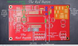
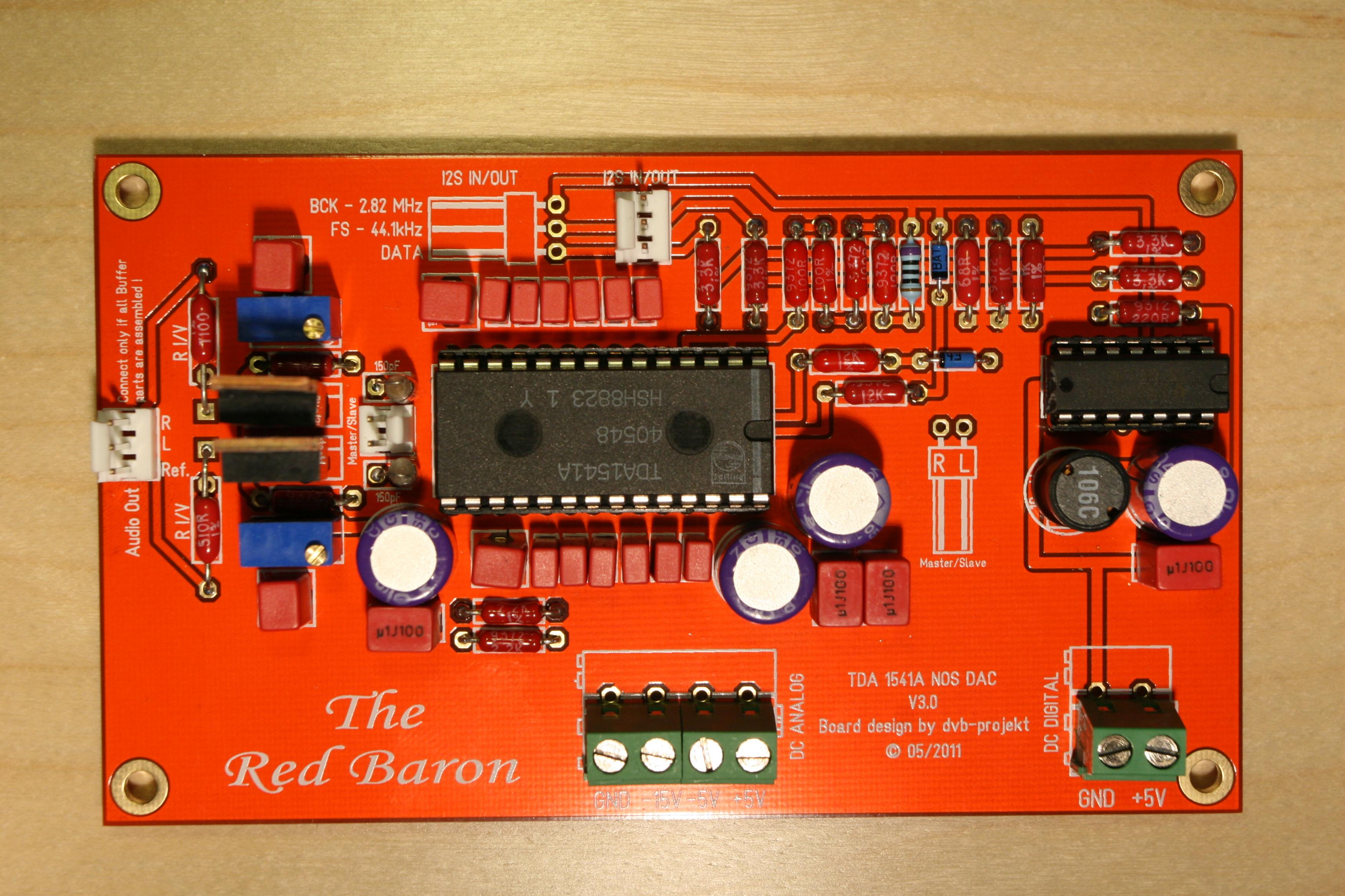
On the Red Baron PCB, is there any downside to substituting the Nichicon FPCAP R7 150µf/16V for 220uf/16v caps?
Thanks
On the Red Baron PCB, is there any downside to substituting the Nichicon FPCAP R7 150µf/16V for 220uf/16v caps?
Thanks
Next try to get red baron to fly
as a follow up to my post http://www.diyaudio.com/forums/grou...dac-i2s-bus-architecture-151.html#post4718234
I finally managed to get some time to try to get red baron to fly again by re-configuring it to run in I2S mode and connecting it directly to the I2S outputs of Ian's clock board.
It does not work and I suspect that the reason for it is that there is something wrong with 1N4148 diods.
There is a nice signal going in to diods from WS/LE and DATA/L u.fl sockets:


and on the other side of the diods the signals (without changing the scope settings) look like this:
.jpg")

Can anyone provide a scope view on the diod outputs, or the WS DATA/L TDA inputs for comparison?
Any hints on what could cause this signal change apart from obvious - broken diods?
as a follow up to my post http://www.diyaudio.com/forums/grou...dac-i2s-bus-architecture-151.html#post4718234
I finally managed to get some time to try to get red baron to fly again by re-configuring it to run in I2S mode and connecting it directly to the I2S outputs of Ian's clock board.
It does not work and I suspect that the reason for it is that there is something wrong with 1N4148 diods.
There is a nice signal going in to diods from WS/LE and DATA/L u.fl sockets:
and on the other side of the diods the signals (without changing the scope settings) look like this:
Can anyone provide a scope view on the diod outputs, or the WS DATA/L TDA inputs for comparison?
Any hints on what could cause this signal change apart from obvious - broken diods?
Any hints on what could cause this signal change apart from obvious - broken diods?
Digital audio is highly problematic. I spent much time attempting to get best sound out of a multibit chip. Sound quality is inconsistent, one day it sounds quite well, the other day it is not that great.
We have a D/A converter that basically converts a number into a corresponding voltage or current. The TDA1541A outputs a current.
Circuits and components are not perfect so we have crosstalk.
The major problem with every DAC chip is loading the data without causing too much unwanted interference on the DAC output.
PWM signals (varying duty cycle) generate a varying average voltage. This way we can vary the output voltage of a SMPS or control the speed of motors for example.
The data signal (part of the I2S / simultaneous interface) does something similar. It’s average DC voltage varies with the data content (music). Here the PWM interaction is highly undesirable as it causes data related distortion.
This varying signal that varies between 0V (no data) and a given maximum value basically injects a varying DC voltage into the DAC chip. This ac voltage has a spectrum that varies with the data content.
Because we are using imperfect components and circuits on the chip, this data interference seeps through the DAC chip circuits and appears at the output (attenuated of course).
The impact causes major sound quality degrading. With repetitive test signals (sine wave) the impact of this data distortion is limited and all seems fine (SNR is ok). This changes drastically when feeding complex audio data into the same chip as the spectrum gets way more complex and non repetitive.
In order to reduce this digital interface flaw we can do a number of things:
-> Attenuate the I2S signals to lowest possible levels where the DAC chip still triggers reliably.
-> Limit the data run length.
With standard I2S and 24 bits data we have data activity (and interference) during 48 of the 64 bits in a frame. This is pretty high, 64 bits of activity on a 64 bit frame would give 100% data related distortion. In this case (48 bits) we have 75% data related distortion.
This also means that 24 bit playback will increase data related distortion by 12.5%. So 16 bits data causes less data related distortion, very important to know when streaming 24 bit files.
So when streaming 24 bits with the idea of getting more resolution and refinement we are actually boosting data related distortion by 12.5%. I doubt if the extra bits will have any advantage when swamped by increased data related distortion.
Similar, S/PDIF causes high data related distortion too, it approximates 100%.
With 16 bits data we have activity during 32 of the 64 bits in a frame so 50% data related distortion.
With 16 bits simultaneous mode we have activity during 16 of 64 bits or 25% data related distortion. This is why simultaneous mode sounds better than I2S mode as data related distortion is halved.
In the discrete Mosaic D/A converter I designed I use multiple 8-bit data channels (multi-stream interface) so I can load all data while having activity during 8 of the 64 bits. This reduces data related interference to only 12.5%. The resolution doesn't matter now because I can clock in 24 bit data with the same 8 bit data activity as I use multiple serial data channels simultaneously.
Modern DAC chips clock data continuously (oversampling, delta sigma modulator) and always have close to 100% data related distortion.
With TDA1541A we could reduce data related distortion to 12.5% by combining two TDA1541A chips with ratio 1:256 or load the 8 MSBs into one chip and the 8 LSBs into the second chip, then connect both outputs together and perform full-scale trimming when necessary.
So like this:
TDA1541A #1 -> D15, D14, D13, D12, D11, D10, D9, D8, 0, 0, 0, 0, 0, …….
TDA1541A #2 -> 0, 0, 0, 0, 0, 0, 0, 0, D7, D6, D5, D4, D3, D2, D1, D0, 0, 0, 0, 0, ……….
So we only have 8 bits data activity. When using I2S instead of simultaneous mode we would need 4 TDA1541A chips as we could only use one channel of each chip.
Another way to reduce data related interference is reducing data signal amplitude, thus reducing its energy. There are however limits to this, at some point the DAC chip will no longer trigger or triggering gets unreliable.
This is achieved with the diode attenuator. We should end up with 1V2pp signal instead of 3V3pp or 5Vpp considerably reducing data related interference levels. This is done by using the approx. 0V6 voltage drop of the diodes.
Problem however is that logic circuits only detect signals that swing around a given DC bias voltage or current. Therefore we cannot simply attenuate the signal so it swings between say 0V and 1V2 as the chip simply won’t trigger.
-> The TDA1541A requires a DC bias voltage of approx. 1V2, logical “1” would then be 1V8 and logical “0” 0V6.
The problem however is that there are tolerances in diode voltage that also depend on temperature and diode current.
-> Higher diode temperature -> lower voltage drop.
-> Higher diode current -> higher voltage drop.
We need the temperature dependency of the diodes in order to compensate temperature dependency of the trigger circuit inside the TDA1541A. It would also be best to thermally couple all attenuator diodes with the TDA1541A.
-> So you have to play around with diode bias current and this can be done by varying the value of the pull-up series resistor that sets the current running through the diode string. Lower pull up resistor value means more bias current and higher voltage drop.
Because you don’t know if only one or more inputs are not responding it is best to connect all inputs directly to the 3V3 or 5V I2S input signal (disconnecting the attenuator!). Now you should have sound.
Next re-connect the diode attenuators one by one. If the sound stops or gets distorted you have to change the value of the pull-up resistor until it works reliably. Repeat this for all attenuators.
I would test the minimum and maximum series resistor value where the DAC is no longer triggered, say 1K and 4K. Next I would pick a resistor value that’s exactly between these extreme values, in this case 2K5.
Hope this helps.
Thanks a lot for the great explanation of digital interface flaw and the roadmap to get the attenuator circuit to work!
Last edited:
Regarding the choice of capacitors in the BOM for red baron 5.
The statement :
Quote : If you could solder SMD, use the Cornell Dubilier 1µF/16V FCA 1210 caps
on all active divider decoupling positions – Mouser Part No.: 598-FCA1210C105M-G2
or SMD Cornell Dubilier 2.2nF/50V FCP 0805 cap – Mouser Part No.: 598-FCP0805H222G-J1
Unquote
I presume the Cornell Dubilier 1µF/16V FCA 1210 caps
on all active divider decoupling positions – refers to caps for decou 1 to decou 14 positions ??
In the schematic , it states to use 220nf except for C7 and C8 where 1Uf is specified .
thanks for clarification
kp93300
Regarding the choice of capacitors in the BOM for red baron 5.
The statement :
Quote : If you could solder SMD, use the Cornell Dubilier 1µF/16V FCA 1210 caps
on all active divider decoupling positions – Mouser Part No.: 598-FCA1210C105M-G2
or SMD Cornell Dubilier 2.2nF/50V FCP 0805 cap – Mouser Part No.: 598-FCP0805H222G-J1
Unquote
I presume the Cornell Dubilier 1µF/16V FCA 1210 caps
on all active divider decoupling positions – refers to caps for decou 1 to decou 14 positions ??
In the schematic , it states to use 220nf except for C7 and C8 where 1Uf is specified .
thanks for clarification
kp93300
Use the Cornell Dubilier 1µF/16V FCA 1210 caps
on all active divider decoupling positions (1-14).


Hi Ya gents,
sort of a newbee question here!.Sorry to bother but i am sorta stuck😕.
On my CDPro 2 I can locate the 12 s output connector- a 6pin effort- so i made a colour coded lead to fit-- with the mechanism on the floor and as i look at it square on from left to right , according to the Phillips data sheet :
Pin 1= Misc (N/c on my lead)
Pin 2 = SCLK (Black on my lead)
Pin 3= WCLK (Brown on my lead)
Pin4= DATA (Red on my lead)
Pin5= Gnd ( Orange on my lead)
Pin6= graphics o/p (N/c on my lead)
Now looking at the Red Baron DAC input: 12S Ground is self explanatory
DATA is also self expansionary
However Sclock (from the CD Pro2) is that BCK or FS on the Red Baron I/P?
Also FS, (from the CD Pro2) is that BCK or FS on the Red Baron I/P?
Any help accepted, as i have yet to hear music from the Red Baron (but i know its in there somewhere!)
Thanks Gents
Johnny
Hi Johnny,
Not a bad question at all.
I pulled this from the Wikipedia article on the I2S standard:
The bus consists of at least three lines:
1. Bit clock line
2. Word clock line - also called word select (WS) or left right clock (LRCLK)
3. At least one multiplexed data line
So it sounds like on your board the SCLK should be connected to BCK on the Red Baron. Though I just looked on my twisted pear receiver board and it has both an SCK and a BCK output and I use the BCK. Not sure why?
Here is a Phillips paper on the I2S specification:
https://www.sparkfun.com/datasheets/BreakoutBoards/I2SBUS.pdf
I hope this has been of some help 😱
Thanks for the reply robots
Thank for that, I shall follow this up as I have just bagged a lampizator SRPP pcb and will cobble that to TDA1541 ( as soon as I get a real TDA chip and an instruction sheet for the lampizator PCB on how to populate it) then conjugate that to my Phillips cd pro 2 ( I hope😀)
Thanks again robots
Thank for that, I shall follow this up as I have just bagged a lampizator SRPP pcb and will cobble that to TDA1541 ( as soon as I get a real TDA chip and an instruction sheet for the lampizator PCB on how to populate it) then conjugate that to my Phillips cd pro 2 ( I hope😀)
Thanks again robots
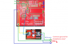
Hi all,
Came back with a question, now, that I've (finally) finished Red Baron, I want to feed my headphone amp with it.
What I've did:
I've set 0V vs. Digital GND via potentiometers.
I've wired the reference module to Red baron as in picture.
I've set the 0V to RCA outs via potentiometers on the reference module board.
What I want is to feed a headphone amp via 3.5mm jack.
In this case the both ground will be linked together.
Will that be a problem? I've found around 1.5V between both RCA out grounds...
Kind rgs,
Alex.
Attachments
It should not be a problem.Anyone please correct me if I am wromg here.
If you check the schematics. All the signal grounds are usually commected together.
So it will happen regardless of the connectivity type you are using rca or headphone jack.
Sent from my ONE A2003 using Tapatalk
If you check the schematics. All the signal grounds are usually commected together.
So it will happen regardless of the connectivity type you are using rca or headphone jack.
Sent from my ONE A2003 using Tapatalk
Having some issues setting up the Red Baron.... I have -0.8V on both L and R channels to GND, playing with the pots does almost nothing. Any ideas? I don't know what the hell I'm doing.
http://imgur.com/AtvyVjP
http://imgur.com/AtvyVjP
Hi all,
Came back with a question, now, that I've (finally) finished Red Baron, I want to feed my headphone amp with it.
What I've did:
I've set 0V vs. Digital GND via potentiometers.
I've wired the reference module to Red baron as in picture.
I've set the 0V to RCA outs via potentiometers on the reference module board.
What I want is to feed a headphone amp via 3.5mm jack.
In this case the both ground will be linked together.
Will that be a problem? I've found around 1.5V between both RCA out grounds...
Kind rgs,
Alex.
Hi Alex,
in this post http://www.diyaudio.com/forums/grou...dac-i2s-bus-architecture-152.html#post4765880 dvb-project says to connect the gnd of the dc reference module to digital gnd. Not sure why, but hope this helps.
Having some issues setting up the Red Baron.... I have -0.8V on both L and R channels to GND, playing with the pots does almost nothing. Any ideas? I don't know what the hell I'm doing.
Imgur: The most awesome images on the Internet
You made a failure with the I/V Resistors.
Please solder the 2nd end of the resistor to the quadrangle solder point like here on an older RB V3.0!
The round solder point vis-á-vis is for the form factor of i.e. TX2575 naked bulk foil resistor.
Best,
Oliver
Hi Oliver!
And for me, does the schematic looks OK? 😀 I didn't shunted the I/V res. when soldered.
Still can't figure what would I do with two different voltage GND from DC ref. board common in the 3.5mm jack for headphone amp.
When I common I get different readings for DC voltage vs. when I measure each channel with it's own GND.
Kind rgs,
Alex.
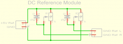
reference dc module
In the ground reference module, there are two outputs----GND REFERENCE L and GROUND REFERENCE RIGHT .
Why do i need two Gnd reference output as the output ground of both channels from the red baron are tied together on the Red baron board ?
Thanks for clarification
In the ground reference module, there are two outputs----GND REFERENCE L and GROUND REFERENCE RIGHT .
Why do i need two Gnd reference output as the output ground of both channels from the red baron are tied together on the Red baron board ?
Thanks for clarification
Attachments
- Status
- Not open for further replies.
- Home
- Group Buys
- "Reference" TDA1541A DAC with I2S-BUS architecture