Hello Atiq,
the parallel circuit of C2 does not sound good. I have all kinds of electrolytic capacitors there now and I also bought the MUSE. A single Muse sounds good - just like Tibi has - two 220uF/25V in series sound better. So I have touched the layout again and enlarged the footprints.
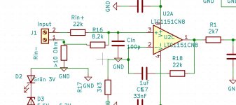
At the input there are now Rin+ and Rin-. It's up to you to decide whether you want to solder wire or resistors. I want to experiment with it to test whether a resistor between GND and input (-) has an effect and what effect.
Regards Tim
Tim, can u pls post a matching schematic? Is this for ground loop break? Thx
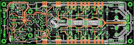
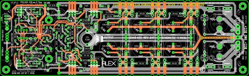
This time, a more relaxed layout , the version, that also fits, larger parts, connections for the version with Mosfet 2SK1058 and 2SJ162 or EPXICON transistors. MUSE capacitors in series, the inductor being a classic one. 🙂
Regard,
Alex
Regard,
Alex
Attachments


This time, a more relaxed layout , the version, that also fits, larger parts, connections for the version with Mosfet 2SK1058 and 2SJ162 or EPXICON transistors. MUSE capacitors in series, the inductor being a classic one. 🙂
Regard,
Alex
Very nice work master!
This time, a more relaxed layout , the version, that also fits, larger parts, connections for the version with Mosfet 2SK1058 and 2SJ162 or EPXICON transistors. MUSE capacitors in series, the inductor being a classic one. 🙂
Regard,
Alex
Hello Alex,
I find your layout very interesting, although I would never do it that way. I do not want to make a fundamental debate here, I see that there are different priorities in the layout creation and the question of ground planes, scattering and mass conductors are evaluated very differently.
I would be really surprised if you can hear a difference between 100uF BP and 2x 220uF BP as C2 when using a MKS as C7. That would disturb my physical world view. The Q17 is a very simple and very functional amplifier with the MKS, so there are also no problems with oscillation, less good speakers...
Regards Tim
Alex,
The layout looks great, I see you do not have protection diodes between the rails and earth and also not gate protection diodes. Also, I suppose the output coil and resistor will be mounted on the speaker connectors ?🙂
The layout looks great, I see you do not have protection diodes between the rails and earth and also not gate protection diodes. Also, I suppose the output coil and resistor will be mounted on the speaker connectors ?🙂
Very nice work master!
Thank you thimios .🙂
@Vrystaat I just follow schematic , don't need protection diodes between rails. Mosfet are protected already .
@Tim 1999de , thanks I'll let you know when I'm testing if I hear some difference regarding BP capacitors .
Last edited:
Alex,
True, the mosfets has a protection diode between source and drain but a zener between drain and gate will protect the gate from being overdriven . It's just a thought.😉
Plse let us know how this baby sounds !😀
True, the mosfets has a protection diode between source and drain but a zener between drain and gate will protect the gate from being overdriven . It's just a thought.😉
Plse let us know how this baby sounds !😀
Nice work Alex !
I would increase C20ab and C25ab to 330uF-470uF or even more with the price of a larger pcb. This will lead to more space between final transistors which is also desired for better thermal dissipation.
Regards,
Tibi
I would increase C20ab and C25ab to 330uF-470uF or even more with the price of a larger pcb. This will lead to more space between final transistors which is also desired for better thermal dissipation.
Regards,
Tibi
Last edited by a moderator:
Jan,
You may add zener between gate and source. As I already mentioned, this will protect only in case of Q5 and Q6 failure. On other hand, this will add Vgs modulated parasitic capacity which is not desired.
However, if you still want to have one, a 9,1V zener may be added before gate stoppers, only one.
Regards,
Tibi

I would not recommend anti clip diodes. These will considerably degrade performance.
However, when you design a commercial product, you must take care on any possible damage a "dumb" user may do, at the cost of performance and price.
I do not think such extra care should be considered in our case. Even in your schematic there is a jumper, indicating that a normal user may remove this protection.
Regards,
Tibi
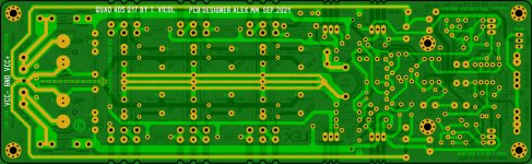
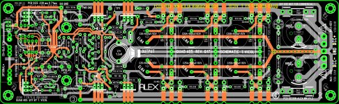
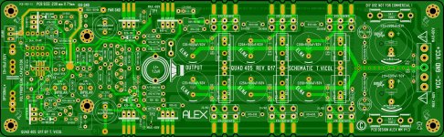
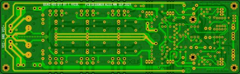
Size of PCB now 230 mm x 71mm . I hope no errors on board . I will check tomorrow again .Thanks Tibi , good tips with larger elcos and biger distance OT .🙂
Regards,
Alex
Regards,
Alex
Attachments

Got a stupid question. I was looking at the schematic, seems like there's no adjustment for bias and DC offset, correct me if I'm wrong. Is there a build instructions how to power up this amp slowly to make sure everything is good? Sorry, I'm not an expert.
fredlock, it is a good question. Already addressed, but I'll try to add some more info.
Q17 in running mainly in class B with negligible AB operation. There is no need for bias adjustment, unless you use lateral mosfet or some other vertical mosfet with different Vgs threshold.
In case of Exicon laterals R11 and R12 = 10ohm.
Q12 & Q6 form a ccs. If you still want to slightly adjust bias, this can be achieved by changing ccs current trough R13. A series 22ohm multiturn potentiometer + 5ohm resistor may replace R13. This way you can adjust current trough class A stage, formed with Q5 and Q6. Together with ccs current the bias voltage over R11 and R12 will have a variation, changing final stage operation. For symmetry, R10 must mach pot+5ohm.
Please also note, if you want thermal tracking, Q12 need to be mounted on heatsink. Q12 Vbe is the main ccs voltage reference.
DC offset is achieved trough servo with R23+R17+C2.
More details at Q17-a-QUAD405-audiophile-approach/Q17.pdf at main * tvicol/Q17-a-QUAD405-audiophile-approach * GitHub
Regards,
Tibi
Last edited by a moderator:
Thanks. Alex, can you pls add a dual op-amp option?
Dual opamp implemented on board . 😉
Regards,
Alex
Attachments
Hello Atiq,
You can tell us soon how the two layouts perform? I suppose you're going to build Alex's board too, right?
That's great, I'm very curious about your report.
You can tell us soon how the two layouts perform? I suppose you're going to build Alex's board too, right?
That's great, I'm very curious about your report.
- Home
- Amplifiers
- Solid State
- Q17 - an audiophile approach to perfect sound