I guess P1 is to adjust the DC offset.
Doesn't adjust anyway is too low one channel -0.010 V the other channel -0.003 V
Adjusted P1 till have 4.24mA across R7 220 ohms but the rest of measurements aren't OK: for example across R2 180 ohms I measured 1.511V so 8.39mA.

Hi,
see attachment for the simulated values with LSK389C Cordell model (Idss: 8.3mA, Vp: -536mV)
Around 8mA through R2 and R7/P1 seem a bit high.
The increased voltage drop leads to an increase of current through the bipolars also.
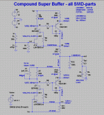
You may want to check the voltage drops over R5, R6,R10 and R11 and calculate the associated currents by I=Voltage drop/Resistance.
If the currents are >>70mA, R6 and R11 should rather be increased, as the heat power losses over Q1 and Q2 might become too large.
jauu
Calvin
see attachment for the simulated values with LSK389C Cordell model (Idss: 8.3mA, Vp: -536mV)
Around 8mA through R2 and R7/P1 seem a bit high.
The increased voltage drop leads to an increase of current through the bipolars also.
You may want to check the voltage drops over R5, R6,R10 and R11 and calculate the associated currents by I=Voltage drop/Resistance.
If the currents are >>70mA, R6 and R11 should rather be increased, as the heat power losses over Q1 and Q2 might become too large.
jauu
Calvin
Attachments
Hi Calvin,
You are very kind doing the simulation and give guidance to adjust your buffer. Yesterday listened all night, compared vs schematic "B" it seems that schematic "C" have steroids🙂
I will try and let you know
Cheers
Felipe
You are very kind doing the simulation and give guidance to adjust your buffer. Yesterday listened all night, compared vs schematic "B" it seems that schematic "C" have steroids🙂
I will try and let you know
Cheers
Felipe
Hi Calvin,
You are very kind doing the simulation and give guidance to adjust your buffer. Yesterday listened all night, compared vs schematic "B" it seems that schematic "C" have steroids🙂
…
It looks like there is a good reason why Calvin evolved his buffer from topology "B" to "C"…
The other channel:
R2 5mA
R7/P1 4.3mA
R5 51mA
R6 54mA
R10 51mA
R11 60mA
DC offset 0.004V
R2 5mA
R7/P1 4.3mA
R5 51mA
R6 54mA
R10 51mA
R11 60mA
DC offset 0.004V
Last edited:
R2 5.2mA
R7/P1 4.3mA
R5 55mA
R6 60mA
R10 55mA
R11 60mA
Can I left R6-11 2R2?
DC offset -0.012V
The other channel:
R2 5mA
R7/P1 4.3mA
R5 51mA
R6 54mA
R10 51mA
R11 60mA
DC offset 0.004V
Initially the results you got look okay. The exact currents are dependent on the master JFETs Idss and the degree of matching between them.
Enjoy listening to music…

Hi,
the numbers in #594 appear ok.
The most important numbers of R6 and R11 are the same.
The second most important numbers of R5 and R10 are the same also.
The last two numbers simply differ, due to the value of R7/P1 beeing just the calculated value of R7´s current.
The numbers in #595 can´t be correct.
There´s a difference between R6 and R11 of 6mA.
As this difference current must flow through the 100k Ballast resistor R12 this would lead to a (theoretical) output offset voltage of 600V(!)
The number of R6 is also quite unbelievable as the current through the bipolar transistors (indicated by R5 and R10) are the same.
The numbers of R2 and R7 are quite similar to those from #594, also not indicating something wrong.
The offset voltage value of -12mV calculates to a current imbalance between lower and upper part of the Buffer of tiny 120nA
Hence I assume a false number for R6 (also 60ma) or/and false numbers for R5 and R10 (54mA).
Around 6mA for the JFETs (54/60mA) seems more realastic than 9mA (51/60mA)
As the output offset is very small all hints to a calculation or measurement error, not to a failure in circuit function.
Merlin, could You measure the voltage drops over those 6 resistors and the output offset again?
jauu
Calvin
Calvin
on your schematic #591 are two possible output transistors: KSA1381 (through hole) or FZT751 (SMT).
Those two parts have different Cob, what about compensation caps C1, C2? Should they be adjusted individually?
on your schematic #591 are two possible output transistors: KSA1381 (through hole) or FZT751 (SMT).
Those two parts have different Cob, what about compensation caps C1, C2? Should they be adjusted individually?
- Home
- Source & Line
- Analog Line Level
- Preamp-Buffers - simple idea