SOT-89 PNP bipolar transistor on collector pin as close as possible to MJL3281 package
This was difficult to solder even with the power transistor off the heat sink, and the MMBT3904 works better.

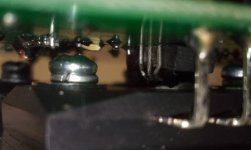
MCP9701A temperature sensor.
This one was in the green curves from all the other plots.
It has two NC pins which can be used as thermal conductors: since they are internally isolated, I connected them to the collector lead on the PCB through a thick copper trace. It has been on the PCB from the beginning, monitoring the temperature of the PNP power transistor, but not the NPN transistor.
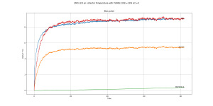
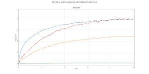
I just realized all the plots say "MJL1302" in the title even when it's the MJL3281 doing the heating. Meh, who cares. The important thing is the plot in the previous post with the BD139 close to the power transistor was using MJL1302 as a heater. Instead of moving the BD139 for both plots, I put it close to one of the power transistors and tested with both.
The important thing is that on that plot, the MCP9701A sensed the temperature of the power transistor through its collector pin faster than the BD139 mounted on the heatsink did.
However applying some gain reveals it has not settled yet at the end of the plot, so while it does sense temperature, it is too slow.

This was difficult to solder even with the power transistor off the heat sink, and the MMBT3904 works better.
MCP9701A temperature sensor.
This one was in the green curves from all the other plots.
It has two NC pins which can be used as thermal conductors: since they are internally isolated, I connected them to the collector lead on the PCB through a thick copper trace. It has been on the PCB from the beginning, monitoring the temperature of the PNP power transistor, but not the NPN transistor.
I just realized all the plots say "MJL1302" in the title even when it's the MJL3281 doing the heating. Meh, who cares. The important thing is the plot in the previous post with the BD139 close to the power transistor was using MJL1302 as a heater. Instead of moving the BD139 for both plots, I put it close to one of the power transistors and tested with both.
The important thing is that on that plot, the MCP9701A sensed the temperature of the power transistor through its collector pin faster than the BD139 mounted on the heatsink did.
However applying some gain reveals it has not settled yet at the end of the plot, so while it does sense temperature, it is too slow.
While we're on the topic of biasing, can anybody shed a light on the bypassing of the bias spreader? I've seen capacitors ranging from 0 to 100's of uF, but when I ask why?, everybody seems to look the other way.
I tried a tiny SOD-123 1N4148.
It doesn't work so well as the BJT, and it doesn't say which leg has best thermal coupling with the chip... With BJTs it's always the collector, and they exist in two polarities, which is convenient.
It doesn't work so well as the BJT, and it doesn't say which leg has best thermal coupling with the chip... With BJTs it's always the collector, and they exist in two polarities, which is convenient.
Attachments

Hi peufeu,
Gee, you would think with the very low thermal mass that an smd diode would have the response would be very quick. You surprised me with this. Could the connecting wire be acting as a heat sink?
-Chris
Gee, you would think with the very low thermal mass that an smd diode would have the response would be very quick. You surprised me with this. Could the connecting wire be acting as a heat sink?
-Chris
Hi peufeu,
Gee, you would think with the very low thermal mass that an smd diode would have the response would be very quick. You surprised me with this. Could the connecting wire be acting as a heat sink?
I think the legs are just very thin so the heat has trouble going all the way. I would like to try with a glass packaged MELF SMD diode because that has short and wide leads, but unfortunately I don't stock these because they love to roll off the table and into the carpet...
Try TO-92 sensor transistor, placed on top of MJL case, centered over the chip, with some thermal grease. It reacts surprisingly fast and is fully isolated..
Alright, great suggestion!
A little bit of difficulty because of the big metal bar squishing the transistors against the heat sink but what the hell, I put them under it and tightened the screws...

2N3904

BD139

They react much faster than the transistor on the heat sink I posted previously, So this really works!
Difference between BD139 and 2N3904 is small enough to not be significant.
BD139 gives a better thermal resistance for the main transistors because it's flat, so I could tighten the screws tight, whether the 3904 is round, so I went a bit more gently...
Last edited:
Now that I think about it, 1N4007 has pretty thick legs for cooling...
Unfortunately this applies to both legs, so without clipping the other one, cooling by random air flow is apparent in the graph as low frequency noise (ie, it doesnt work)

But trimming the other lead short and using very thin wire for wire wrap, then, it works really well! Only a little bit slower than the MMBT3904...

Unfortunately this applies to both legs, so without clipping the other one, cooling by random air flow is apparent in the graph as low frequency noise (ie, it doesnt work)
But trimming the other lead short and using very thin wire for wire wrap, then, it works really well! Only a little bit slower than the MMBT3904...
Another option: the 0805 SMD LED. It is tiny and the body is ceramic, so it should conduct heat pretty well.
It is twice as fast as MMBT3904! I had to change the scale. Also it glows, which is cool.
It is twice as fast as MMBT3904! I had to change the scale. Also it glows, which is cool.
Attachments
Sorry if I missed it, but how exactly did you mount the parts for measuring? I cant quite wrap my head around it =)
Remember the "Thermally enhanced" 2SC5706?

I soldered the LED on it. It works perfectly and tracks the temperature of the copper slug with negligible delay.

Another great data point from this graph is the "15W" maximum dissipation from the datasheet is bogus. It is probably based on the tiny size of the contact area at the back of the transistor, which would imply an embarrassing thermal resistance when using silpad.
But when soldered on a copper slug, it has about 2.5-3°C/W thermal resistance to the copper slug, as shown by the fact its internal Vbe temperature rises almost instantly by 30°C when 12W are applied, but then it follows the temperature of the LED and the copper slug closely.
Apparently I did not tighten the screws well enough in this test, since the temperature of the copper slug keeps rising.
Still this means in a cascode amp these transistors could be biased cleanly and with low value emitter resistors.
I tried an isolated version by adding a layer of kapton tape and copper tape to simulate thermal coupling through the two outer layers of a 4 layer board, but that sucked:

However this time the screws are properly tightened, which means the copper slug transfers heat properly through the heat sink.
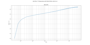
BTW, here's measured transient thermal impedance of the "thermally enhanced" version:
I soldered the LED on it. It works perfectly and tracks the temperature of the copper slug with negligible delay.
Another great data point from this graph is the "15W" maximum dissipation from the datasheet is bogus. It is probably based on the tiny size of the contact area at the back of the transistor, which would imply an embarrassing thermal resistance when using silpad.
But when soldered on a copper slug, it has about 2.5-3°C/W thermal resistance to the copper slug, as shown by the fact its internal Vbe temperature rises almost instantly by 30°C when 12W are applied, but then it follows the temperature of the LED and the copper slug closely.
Apparently I did not tighten the screws well enough in this test, since the temperature of the copper slug keeps rising.
Still this means in a cascode amp these transistors could be biased cleanly and with low value emitter resistors.
I tried an isolated version by adding a layer of kapton tape and copper tape to simulate thermal coupling through the two outer layers of a 4 layer board, but that sucked:
However this time the screws are properly tightened, which means the copper slug transfers heat properly through the heat sink.
BTW, here's measured transient thermal impedance of the "thermally enhanced" version:
Attachments
Metal bar is conducting heat away, slowering desired function. I use it with power transistors fastened with screw. Sensor transistor is pushed with rubber band. So it is not " cooled".A little bit of difficulty because of the big metal bar squishing the transistors against the heat sink but what the hell, I put them under it and tightened the screws...
Last edited:
Sorry if I missed it, but how exactly did you mount the parts for measuring? I cant quite wrap my head around it =)
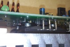
I soldered them where the tweezer points, on the wide part of the transistor collector lead.

This makes a non-isolated temperature sensor, so it is not that convenient.
For the small fast BJTs I mounted the LED (used as sensor) on the copper slug:

This is the isolated version, I didn't take a picture of the non isolated version but it's the same without the insulating tape.
For BV's suggestion...
If you count the legs on the left power transistor, you'll notice there are way too many. That's because there's a BD139 on top.
So, for isolated standard Vbe multiplier, BV's solution of mounting a small transistor on top of the big one works SPECTACULARLY better than bolting the temperature sensing transistor on the heat sink. Since that allows for lower emitter resistors, which allow lower distortion, it will make it sound better.
Metal bar is conducting heat away, slowering desired function. I use it with power transistors fastened with screw. Sensor transistor is pushed with rubber band. So it is not " cooled".
Yes.
I'd drill a hole in the bar or something. But I'm using this heatsink for the test, it has drilled and tapped holes, and I found it with the bar already attached... and the end of my last tap is inside the last heat sink I used it on 😀
Have you tried gluing it with epoxy?
So... while the non-switching topologies would probably look better at unrealistic high frequency/current, will they bring actual benefit?
They do.
First, you ~1.2A output current is not a realistic value for an audio power amplifier. Assuming 1.2A is the peak output current, this would be an output power into a 4ohm load of about 3W, or if it's the RMS current, about 6W. That's low...
Secondly, if you rise the output power, you will note that the frequency to which the crossover mess will vanish is decreasing significantly, because of the strong dependence of bipolar storage time on the collector current. This is to say, that the higher the base current, the higher the amount of charge to be evacuated and/or recombined from/in the transistor base at turn off, per unit time.
Third, the usual rule for non switching output stage is to keep the geometric average of the two halves collector currents constant; that would be Icn*Icp=const at all frequencies of interest. Implementing such a rule would mean that up to the frequency limit, collector current will never become zero, hence the bipolars never turn off, hence the stored charge discussion above becomes, in a first approximation, a moot point. Note the bold above; some people believe that if the collector currents don't cancel at low frequencies that's good enough; it is not. That's one reason why ICs like the LT1166 fail short for the full audio band applications; they simply don't have enough bandwidth to keep the above rule at audio HF (if memory serves from about 10 years ago, the LT1166 is effective only to about 4KHz, being therefore good for a subwoofer audio amplifier).
Implementation of such a non switching wideband circuit is difficult; it requires a nonlinear feedback network, that has it's own stability issues, almost impossible to tame with anything like a regular compensation method. I remember Edmond Stuart simulated such a circuit, which failed short of stability (on my bench, it was experiencing latchup when driving the amp with fast signals) and any stability-bandwidth trade-off was leading nowhere from a practical perspective. I haven't see a solid non switching full solution for the entire audio band, but only partial improvements over the standard solution of an acceleration cap (100nF, in your case), which is not a solution for non switching, but only a bandaid to limit the effect of the crossover mess. Part of this lack of sulutions is of course keeping the complexity within reasonable limits; Edmond's solution mentioned above, in despite of it's stability issues, is already a rather complex circuit, and I don't think anything simpler could be designed and successfully implemented.
Last edited:
They do.
If they work 😀
First, you ~1.2A output current is not a realistic value for an audio power amplifier. Assuming 1.2A is the peak output current, this would be an output power into a 4ohm load of about 3W, or if it's the RMS current, about 6W. That's low...
Levels measured on my speakers, it was pretty damn loud. However they are reasonably efficient (92dB/2.83V/1m).

Secondly, if you rise the output power, you will note that the frequency to which the crossover mess will vanish is decreasing significantly, because of the strong dependence of bipolar storage time on the collector current. This is to say, that the higher the base current, the higher the amount of charge to be evacuated and/or recombined from/in the transistor base at turn off, per unit time.
Yes, definitely.
Once the inductive emitter resistor problem was solved this became apparent. The size of the mess seems related to di/dt at turn off, which is logical: the higher the di/dt, the less time it has to purge stored charge and turn off cleanly.
I was quite surprised by how much trash the drivers make though.
That spawned the bias temperature sensor test, because with a better bias sensor, lower emitter resistors can be used, which means the BJTs keep more of their exponential characteristic through a wider range of current... so they turn off at a higher output current, and hopefully a lower di/dt, and they do much less gm-doubling. But the resulting gm has a big hole in the middle, which causes other problems.
Icn*Icp=const at all frequencies of interest. Implementing such a rule would mean that up to the frequency limit, collector current will never become zero, hence the bipolars never turn off, hence the stored charge discussion above becomes, in a first approximation, a moot point. Note the bold above; some people believe that if the collector currents don't cancel at low frequencies that's good enough; it is not. That's one reason why ICs like the LT1166 fail short for the full audio band applications (...)
+1
I've noticed in simulation. It looks neat at first sight, but man the details are nasty.
On the other hand, MOSFETs deliver a cleaner crossover with flatter gm, and they have no switching issues...
On the other hand, MOSFETs deliver a cleaner crossover with flatter gm, and they have no switching issues...
Surprise, surprise, they do have Gm doubling effects... All mosfets have what is called a "subthreshold conduction" region. This is the region around the threshold gate-source voltage; in this region, the Id=f(Vgs) is exactly as exponential as in a bipolar transistor, the parabolic dependency picks up outside this region. The larger the mosfet, the more extended the subthreshold conduction region (toward higher currents). So at crossovers, mosfets will presend the same type of Gm doubling effect, hence the same type of crossover distortions as bipolars, although to a lesser extend, simply because their transconductance is in general much lower.
However, indeed mosfets do not have a storage time to affect their turn off, charging/discharging the Cgd is not the same as evacuating charge from the bipolar base, so this is indeed an advantage. Some people (including Bob Cordell) prefer to view this phenomena as mosfet devices having a much larger transition frequency compared to bipolar beta(freq); in my book this is physically wrong, since mosfets have completely different conduction mechanisms compared to bipolars, so the "transition frequency" definition for bipolars does not apply, and has no direct equivalent, in mosfets. It's comparing apples and oranges if you prefer.
Not glued, becase of dissasebly, if needed in future...Have you tried gluing it with epoxy?
Only pressed by piece of rubber and conected direct to PCB. I do it according picture.
Attachments
Last edited:
Surprise, surprise, they do have Gm doubling effects... All mosfets have what is called a "subthreshold conduction" region. This is the region around the threshold gate-source voltage; in this region, the Id=f(Vgs) is exactly as exponential as in a bipolar transistor, the parabolic dependency picks up outside this region. The larger the mosfet, the more extended the subthreshold conduction region (toward higher currents). So at crossovers, mosfets will presend the same type of Gm doubling effect, hence the same type of crossover distortions as bipolars, although to a lesser extend, simply because their transconductance is in general much lower.
Yes, but.
Lateral ALFETs (same as Exicon) work quite as you say, you either get gm doubling or a hole in the middle of gm curve, no matter the source resistor value (gm plot). So they cause the same (in fact, more) static high order distortions than bipolars. But I think that's because they don't have
a wide enough exponential subthreshold zone... the gm plot looks like what would happen with two almost ideal square law devices with integrated source resistors that you can't get rid of. Of course getting rid of the source resistors would help, but they're inside the devices.
With vertical FETs like IRFP240/9240 the switch between subthreshold and square law seems to happen just at the right place. With high value source resistor you get gm doubling, but with low value you don't. Gm plot. However transconductance is low so there is a dip in the middle, which means they need quite high bias (100-200mA) to give a nice flat gm. Basically the exponential subthreshold of the FET that is turning off meets the characteristic of the other which is already into square mode, that looks like a happy mix. I like the fact they deliver a gm-doubling free characteristic over a wide range of bias without changing resistor values, which means an adjustable bias amp can be built, with a "waste more power to sound better" knob.
Bipolars for reference.
> Some people (including Bob Cordell) prefer to view this phenomena as mosfet devices having a much larger transition frequency compared to bipolar beta(freq);
Measuring input and output current for IRFP240/9240 gives a current gain-bandwidth product of only a couple tens of MHz so yeah I don't get where he pulls these very high "hundreds of Mhz fT" from.
Last edited:
Fast Auto Bias
A thread started on this here Towards a wideband non switching Auto Bias power amp
Cheers,
Ian
+1cn*Icp=const at all frequencies of interest. Implementing such a rule would mean that up to the frequency limit, collector current will never become zero, hence the bipolars never turn off, hence the stored charge discussion above becomes, in a first approximation, a moot point. Note the bold above; some people believe that if the collector currents don't cancel at low frequencies that's good enough; it is not. That's one reason why ICs like the LT1166 fail short for the full audio band applications (...)
A thread started on this here Towards a wideband non switching Auto Bias power amp
Cheers,
Ian
- Home
- Amplifiers
- Solid State
- Power amp OUTPUT STAGE measurements shootout