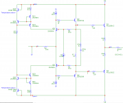
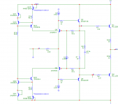
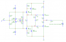
Circuit to be tested.
The sense transistors create a current with an adjustable tempco (via R11,R21) which acts on Q5,Q6 to set the bias. This driver arrangement allows using a large capacitor between the driver emitters, because voltage across it is kept constant by Q5,Q6. Temperature of Q5,Q6,Q11,Q12,Q21,Q22 should be kept reasonably the same.
Spice likes this circuit, we'll see...
Attachments
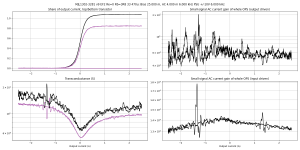
Results: with 10V Vce, bias is stable to the milliamp up to about 350mA, which is exactly what I needed. Also it settles in less than half a second, which is nice for stepping.
OK, all these bias sensor tests are not helping towards the current goal which is to know if there is a point in making an output stage without emitter resistors.
The tests involved do not require correct bias during cooldown, but they do require correct bias during the test, otherwise I'll have no idea what bias I'm testing at, which means fair comparison with MOSFETs will not be possible.
For this I can simply use MMBT3904 soldered on the collector lead as a temperature sensor. So that's what I will do.
Thank you for our dedication, keep up the good work!
I prefer to use the clamping/bar too. I have built some class A amps, and saw the diff temp between output transistors and heat sink go down when I clamped them instead of using screws. It also makes working on the amp easier I think.
If Proton sold budget amps commercially without emitter resistors, it should be doable in DIY. I think a standard bias spreader with good tuning and good thermal coupling could do the job. My 'hack job' on the Proton was pretty close already.
Try simulating the circuit with temperature variations in LTspice and watch the current, I found it can give a pretty good starting point, at least it will tell you what could work and what will make smoke 🙂 Later you can try it IRL and heat it with a heat gun to see what happens, run some transients etc.
Last edited:
It seems to work 😀
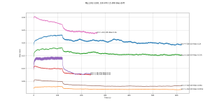
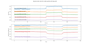
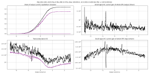
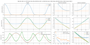
This is the schematic above. Power supplies are +/-10V (except the trace that says +10/25V), and it runs at various biases from 25mA to 300mA. All are stable.
I've connected the output to ground with a 7.5R resistor, and during the first part of the graph it outputs +/-5V, so each transistor heats by about 3W in turn, which is a really tiny 1.5W average per transistor. Then it stops the heating, disconnects the load, and records the cooldown.
I can't really run at higher supply voltage because I need at least one instrumentation amplifier to measure bias on the resistor, which is now on the collector of the NPN.
So I'm going to use the auxiliary MOSFETs to switch a 3.75R load to each rail, which will keep the Vce constant, so each transistor should dissipate 28W with a duty cycle of 50%.
Attachments
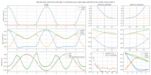
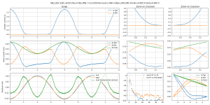
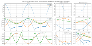
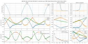
I did a simulation of four bias currents (1 mA, 7 mA, 20 mA, and 50 mA) for the emitter currents.
A ZIP file with the Qucs-S schematics, ngspice simulation, and the results is attached.
Long time Qucs, Qucs-S and QucsStudio user.
I tried replicating your results in Qucs-S but Ngspice crashes.
I see .INCLUDE "C:/Program Files (x86)/Qucs-S/share/qucs-s/xspice_cmlib/include/ngspice_mathfunc.inc" in the netlist. Is this in the Qucs-S schematic? Qucs-S didn't place this in that location on my machine. Can you explain your setup?
Tom
Attachments

Last edited:
Excellent outcome.. thanks for testing many possibilities
Has any tested, OPS with Lateral MOSFETs as drivers and vertical/hex FETs as Output stage instead of BJTs ?
Has any tested, OPS with Lateral MOSFETs as drivers and vertical/hex FETs as Output stage instead of BJTs ?
I did a simulation of four bias currents (1 mA, 7 mA, 20 mA, and 50 mA) for the emitter currents.
A ZIP file with the Qucs-S schematics, ngspice simulation, and the results is attached.
Additional info:
I also downloaded your C300 files from Github. Half work and half cause ngspice to crash. I still haven't figured our why I can't get some of your files to work in Qucs-s/ngspice.
Attachments
HA HA HA HA
Did anyone spot the mistake in the schematic? I swapped 2 parts and it had the tempco in the wrong direction so it helped it run away instead of compensating...
On the positive side, if it didn't explode with double the tempco, it means it wasn't that hard 😀
It works a lot better now...
Fixed schematic:
Attachments
The drivers were warming up the transistors in the circuit, a piece of cardboard as insulator fixed it. Now it works.
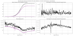
Explanation for measurement below:
First minute, the software tweaks the bias as it settles, so the trace is noisy.
Second minute, it lets the bias settle.
Then it heats the transistors by connecting a 3R75 resistor to one supply then another in turn, and it measures the bias with resistor disconnected.
Then it lets it settle again.
I've adjusted the tempco for clean settling without underbiasing after heating.
Plot on the bottom is the voltage between power transistor bases.
Attachments
I did a simulation of four bias currents (1 mA, 7 mA, 20 mA, and 50 mA) for the emitter currents.
A ZIP file with the Qucs-S schematics, ngspice simulation, and the results is attached.
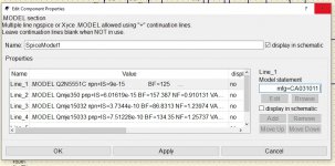
ngspice that I have installed does not like "mfg=CA031011" in 2N5551C model. Text in model is full of spaces or tabs as well.
.MODEL Q2N5551C npn
......
mfg=CA031011
Attachments
Last edited:
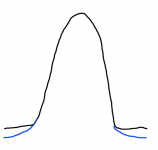
Crossover spikes test on the new resistor-free output stage.
Resistor-free BJTs should behave like vertical MOSFETs with regards to bias: more is better, no gm-doubling. There is a limit, because the internal resistances still exist, but the range of biases without gm-doubling is much wider.
This means an adjustable bias (or adaptive bias depending on the volume setting, or whatever) is possible with both vertical MOSFETs and resistor-free BJTs. But not with BJT+resistors, because then you get gm-doubling, which has the double bonus of worsening both static crossover distortion and turn-off spikes.
Since the goal is to have a wide crossover, and exploit the exponential characteristic of BJTs, I tested it at 200mA bias. I's running and will do the other bias later, if smoke does not happen.
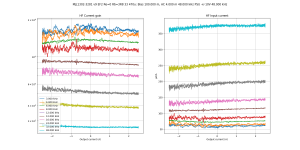
First plot is the only test I could find at 200mA bias of the previous configuration: slow drivers (MJE1503/1) with 17mA bias and inductive emitter resistors.
Second plot is the new resistor-free output stage, with fast drivers (2SC5706/A2039) biased at 36mA.
It only measures the collector current of the NPN, because there was no space to a the current sense resistor on the PNP. But the crossover region, near zero current, is much softer.
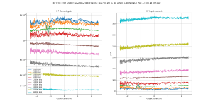
Base currents are quite smooth, but there is still a small bump. This is 24kHz though. It disappears at 12kHz (next plot).
Resistor-free BJTs should behave like vertical MOSFETs with regards to bias: more is better, no gm-doubling. There is a limit, because the internal resistances still exist, but the range of biases without gm-doubling is much wider.
This means an adjustable bias (or adaptive bias depending on the volume setting, or whatever) is possible with both vertical MOSFETs and resistor-free BJTs. But not with BJT+resistors, because then you get gm-doubling, which has the double bonus of worsening both static crossover distortion and turn-off spikes.
Since the goal is to have a wide crossover, and exploit the exponential characteristic of BJTs, I tested it at 200mA bias. I's running and will do the other bias later, if smoke does not happen.
First plot is the only test I could find at 200mA bias of the previous configuration: slow drivers (MJE1503/1) with 17mA bias and inductive emitter resistors.
Second plot is the new resistor-free output stage, with fast drivers (2SC5706/A2039) biased at 36mA.
It only measures the collector current of the NPN, because there was no space to a the current sense resistor on the PNP. But the crossover region, near zero current, is much softer.
Base currents are quite smooth, but there is still a small bump. This is 24kHz though. It disappears at 12kHz (next plot).
Attachments
-
 scope-Bias=200.000 mA Iout=2.560 A F=24.000 kHz MJL1302-3281 v6 EF2 Re=0R33+4R7 Rb=3R8--MJL1302-.png278.2 KB · Views: 402
 -
 scope-Bias=200.000 mA Iout=2.560 A F=24.000 kHz MJL1302-3281 v8 EF2 Re=0 Rb=3R8--MJL1302-3281 v8.png253.7 KB · Views: 395
 -
 scope-Bias=200.000 mA Iout=2.560 A F=12.000 kHz MJL1302-3281 v8 EF2 Re=0 Rb=3R8--MJL1302-3281 v8.png263.1 KB · Views: 391
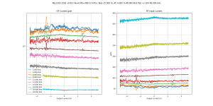
So is it perfect? No!

At lower bias currents, the crossover spikes are small, but they're still there, in the input current...
At lower bias currents, the crossover spikes are small, but they're still there, in the input current...
Attachments
Two problems:
I said an advantage of this topology is it should be able to work with a large capacitor between driver emitters. It should also be able to work without it, so I tried it, and...
Problem #1: without the capacitor, I got some sort of strange latch-up, the output signal was basically a square wave.
I don't see exactly how that would happen from the schematic, and spice doesn't help. But syn08 said he also experienced similar latch-up issues with AutoBias2. Got any idea?
Problem #2: with the capacitor in, if I increase the bias too fast (from zero to the preset value) it also latches up at full bias. But if I increase the bias slowly, it works fine. That's probably the same root cause.
Last edited:
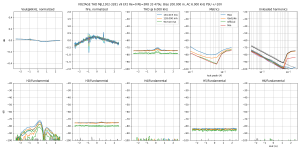
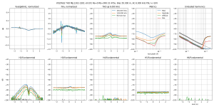
I ran the distortion test anyway, at various biases.
Current gain is excellent, flat over the range of output current.
At 25mA bias, Gm has a dip around zero current, but it improves at 50mA and disappears at 100mA. 200mA brings no noticeable improvement. There is no gm-doubling thus, like with vertical MOSFETs, bias could be adjusted depending on circumstances, volume, etc.
Harmonics 4 and 6 are much lower than with emitter resistors, the result is quite spectacular. As for 3 and 5 there seems to be a constant distortion that depends on input voltage but not output current. It is not in the source signal, and I have no idea where it comes from. It's annoying, because it obscures the harmonics that would be there.
--/--
Attachments
-
 incurrent--MJL1302-3281 v9 EF2 Re=0 Rb=3R8 33 470u-B=100.0m,HA=4.0m,LA=2500.0m,THDF=6000,12000.png321.7 KB · Views: 119
 -
 incurrent--MJL1302-3281 v9 EF2 Re=0 Rb=3R8 33 470u-B=50.0m,HA=4.0m,LA=2500.0m,THDF=6000,12000.png327.2 KB · Views: 115
 -
 incurrent--MJL1302-3281 v9 EF2 Re=0 Rb=3R8 33 470u-B=25.0m,HA=4.0m,LA=2500.0m,THDF=6000,12000.png308.6 KB · Views: 120
 -
 thd-F=6k-MJL1302-3281 v9 EF2 Re=0 Rb=3R8 33 470u-B=200.0m,HA=4.0m,LA=2500.0m,THDF=6000,12000.png207.2 KB · Views: 126
 -
 thd-F=6k-MJL1302-3281 v9 EF2 Re=0 Rb=3R8 33 470u-B=100.0m,HA=4.0m,LA=2500.0m,THDF=6000,12000.png201.8 KB · Views: 116
 -
 thd-F=6k-MJL1302-3281 v9 EF2 Re=0 Rb=3R8 33 470u-B=50.0m,HA=4.0m,LA=2500.0m,THDF=6000,12000.png215.6 KB · Views: 125
 -
 thd-F=6k-MJL1302-3281 v9 EF2 Re=0 Rb=3R8 33 470u-B=25.0m,HA=4.0m,LA=2500.0m,THDF=6000,12000.png253.9 KB · Views: 136
I think there still is a driver heating the bias transistors problem, because the 200mA bias really looks like 100mA. I checked while it was running on 25-50-100mA then I went off to do something else while it ran, so I know 25-50-100 are legit, but for 200, who knows.
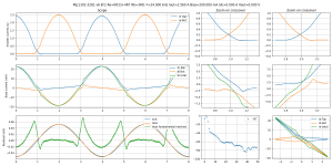
Tthe flat gm curve gives the answer I wanted:
- Gm value is huge, ~10S at 100mA bias, and it is very flat, which results in very low high order distortion. That's awesome.
- The current span of the crossover zone is also huge. I only put a resistor in the NPN collector to measure its current, so the the top left graph doesn't show the PNP current, but with 100mA bias it gives about 1.5A of class A which is also awesome. Unless speaker efficiency is very low, this is essentially a non-switching output stage.
However.
The two spikes spotted previously on the scope also appear. But they do not happen at power transistor turn-off. They happen at lower current. This means there is something wrong with this topology.
However, the resistor-free BJTs score a huge win here 😀
They will need another topology though, and it has to ignore driver Vbe otherwise bias stability without resistors will get a lot more... interesting.
Maybe CFP drivers.
But will they win against the MOSFETs?
Attachments
-
 gm-F=6k-MJL1302-3281 v9 EF2 Re=0 Rb=3R8 33 470u-B=25.0m,HA=4.0m,LA=2500.0m,THDF=6000,12000.png223 KB · Views: 128
 -
 gm-F=6k-MJL1302-3281 v9 EF2 Re=0 Rb=3R8 33 470u-B=50.0m,HA=4.0m,LA=2500.0m,THDF=6000,12000.png221.3 KB · Views: 119
 -
 gm-F=6k-MJL1302-3281 v9 EF2 Re=0 Rb=3R8 33 470u-B=100.0m,HA=4.0m,LA=2500.0m,THDF=6000,12000.png239.8 KB · Views: 115
 -
 gm-F=6k-MJL1302-3281 v9 EF2 Re=0 Rb=3R8 33 470u-B=200.0m,HA=4.0m,LA=2500.0m,THDF=6000,12000.png240.1 KB · Views: 113
I will now try this schematic. The only reason for the weird two-transistor multiplier on the left is that it is compatible with the adjustable-tempco current source that I made earlier. But the important thing is that the drivers' temperature is not part of the equation, only the predrivers. It will also have much more current gain, as a bonus.
Idle current should be chosen such that the drivers never turn off, because CFP turn-off is ugly.
Due to the low output impedance of the CFP, there should be low enough voltage variation on the big capacitor between power transistor bases, so it should be able to stay in.
Idle current should be chosen such that the drivers never turn off, because CFP turn-off is ugly.
Due to the low output impedance of the CFP, there should be low enough voltage variation on the big capacitor between power transistor bases, so it should be able to stay in.
Attachments
It oscillated wildly. Turned out it was the instrumentation amplifier probes on the CFP bases. So, I will measure the base current of the power devices, and the input current of the whole output stage instead: probing there does not cause problems.
Due to... unfortunate circumstances... one instrumentation amp has ben slapped with +25V while it was not powered, so 10V over its input protection spec. Looks like it has gained 30mV offset from the experience...
It seems to work, no oscillations. Looking good so far, 2.5A at 24kHz is very clean. Base currents are from the power devices, they behave just like they did when they had no drivers and just a 470µF capacitor on the base, so that driver is pretty low impedance. I have not put the capacitor between the driver emitters yet. Input current is not displayed here.
Attachments
Last edited:
I dealt with stability and other issues with this type of topology here:
Alternative buffer topologies
Alternative buffer topologies
Thanks, it was an interesting read that resulted in a few new ideas 😀
I see a trend: these schematics with input through the emitters seem finicky. syn08 got it to latch up, I got it to latch up (fortunately the bench power supplies tripped and saved the devices) and you blew an amount of 3055s...
The CFP drivers however seem very stable, oscillation was due to the wires going to the instrumentation amplifier ; I should have put a termination resistor on them from the beginning... but since I'm more interested in the input current of the whole thing than on the input current of each device, I'm fine with not connecting the test leads anyway.
I'm going to see how far this resistor-free output stage can go. Since the base resistors make the transistors turn off earlier just as emitter resistors do (divided by hFe) I will try replacing them with ferrite beads. That should push the turn-off to higher output current.
These non-switching output stages do prevent turn-off (if they work) but in the end, they emulate the gm of an ideal bipolar stage. This means below 100mA bias or so there will always be a hole in the middle of Gm near zero current, so they will have to run at 100mA anyway to get flat gm. So, if it is about emulating the Gm of a pair of bipolars, why not just use a pair of bipolars without resistors? Once the thermal issues are dealt with, which is done, it's pretty simple. They seem to be delivering a smooth and quite pure exponential crossover, and in the measurement above, the one whose Ic is measured was still on with a pretty huge output current...
So, at this bias current, how far can a basic bipolar output stage go before one of them turns off? If that's far enough, maybe non-switching is not actually needed. And the basic topology has a large advantage on bandwidth, which is a requirement for the next stage of this project.
In fact, the current that is kept on the device that does not turn off results in a sharper loss of transconductance for this device: even if it does not turn off, it is still out of the game, pretending to be off, so its transconductance becomes zero (black on the Ic fingerpainted curve below). But if it was allowed to use this extra current margin to turn off smoothly (blue) that would result in a smoother crossover. So, non-switching is a tradeoff: for the same static crossover distortion than a resistor-free BJT output, it needs more bias, but it makes no spikes.
Attachments
Last edited:
- Home
- Amplifiers
- Solid State
- Power amp OUTPUT STAGE measurements shootout