bad idea. You will get what you payed for.😱Guys ngspice isn't the topic, you can do that via PM.
Reichelt sells a ton of Chinese clones of mythical Japanese transistors at pretty cheap prices.
I'm going to order a few.
Reichelt sells per type nr, and has no disclaimers, so what is there to fear. Return to sender in case they do not meet the specs: imo it is then Reichelt's and not your problem.
Can you give me some type # examples: I have some in my stash, but I don't know which ones you prefer
Not the darlingtons... I tried these and was disappointed.
I'm interested in turn-off behavior to get rid of these spikes, so that would be the faster ones preferably. I will look at the datasheets tomorrow.
bad idea. You will get what you payed for.😱
It is not a risky bet considering the price...
Security Check
Reichelt sells per type nr, and has no disclaimers, so what is there to fear. Return to sender in case they do not meet the specs: imo it is then Reichelt's and not your problem.
Yes, and the clones have datasheets that look legit, and the name of the manufacturer is specified... unlike aliexpress where you will get a repackaged 741 that did not meet spec...
---
I think I know why 2SA2039/2SC5706 drivers delivered much better turn-off spikes than MJE15030/15031:
When it is time to turn off the power transistor, output current is low so drivers run at a low current, close to idle, even below idle for the one which drives the transistor that is turning off. That means their fT will be lower. fT depends on current, and the value specified in the datasheet is spec'd for a certain current. But there is usually a graph too.
2SA2039/2SC5706 have fT > 100MHz from 10mA to 1A.
MJL15030/1 does not spec fT at low current, the graph stops at 100mA. But at 10mA, Cordell's spice model gives a fT of only 8MHz. That's 12 times slower.
Therefore, an important point on the shopping list for drivers would be: it should keep a high fT at a current close to the idle current. This means low input capacitance, because at the low end of current, fT comes from gm/C. The requirement of being fast at low current (small chip) conflicts with the other important requirements of having flat hFe at high current and good thermals.
So, perhaps a transistor optimized for fast switching. 2SC5706/2SA2039 are specified for "high current switching, dc/dc converters". That doesn't prevent them from working very well in linear applications, but the low capacitance and high speed means the chip is tiny so the thermals suck, which means they need to be cascoded or bootstrapped.
Bimo's favorites, 2SC517/2SA1930 have 200MHz fT but it is specified at 300mA and there is no graph.
MOSFETs used as drivers would work but they need high Vds otherwise the input capacitance increases a lot, so we get bootstrapping again. The transconductance is still low at a reasonable current though.
CFP drivers can be made very fast and high transconductance, so they have an advantage, also this means they will probably work with a big cap between the driver emitters, so both drivers can work on turning off that transistor.
Last edited:

Proton used 2SA1186/2SC2837 outputs in their amps without emitter resistors, so that could be a suggestion. From memory not so linear at high currents, but pretty fast. Or are you only talking drivers?
How about 2SB649/2SD669 for drivers?
How about 2SB649/2SD669 for drivers?
Last edited:
2SA1186/2SC2837 are NRND but they're pretty fast so yeah it would be interesting to see if they have less turn-off spiking.
After looking at some datasheets, if possible I'd like to try one pair among these, for high fT at low current (will that speed up turn-off?):
2SA1694 2SC4467
2SA1695 2SC4468
and one pair among these, for excellent hFe and fT at high current:
2SA1303 2SC3284
2SA1386 2SC3519
Your drivers are hard to find... also not enough hFe at high current.
CFP drivers have much lower output impedance and better frequency response than darlington drivers (ie, triple).
Lower output impedance means the whole output stage gets smaller gm hole near zero current for the same bias.
Lower output impedance means the whole output stage gets smaller gm hole near zero current for the same bias.
Are the crossover spikes an actual problem?
Here are some measurements on my speakers at pretty loud levels. They are 92dB at 2.83V, 1m ; 8 ohms in the mid-treble and 4 ohms in the bass.
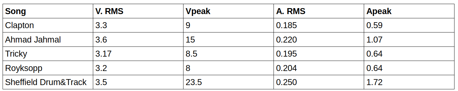
I will take some safety margin and go with 40V peak. An analysis of track "6-Jim Keltner" from Sheffield Drum&Bass...
View attachment 971732
This is a simulation. I oversampled it 4x prior to running the stats.
Left plot is a histogram of amplitude (range 0-1) ; y axis is number of samples at that amplitude. This track has high dynamic range, most samples are close to zero, and about 80 clipped samples.
Middle plot shows a histogram of di/dt in a 4R resistive load with the volume cranked up to 40V peak. There are only ten samples above 0.4A/µs slew rate, so I'll pick that value.
Right plot is a 2D histogram that shows that high slew rate occurs mostly around zero, which is expected.
Here are the places where it happens.

This is the hihat, so it is very quick and there is no warning. This means any mechanism to increase the bias that is based on self-heating of output devices will act too late and only waste power without providing benefit.
A value of 0.4A/µs corresponds to a sinewave of 24kHz at 2.4A peak, that is why I've been testing for spikes around these unexpectedly high values.
Top is RMS power, bottom is highest di/dt at that time.

Closeup

Considering that:
- In that sim, peaks below 0.2A/µs are frequent, but above that, they're pretty rare.
- this is a simulated 4R resistive load, my real speakers are 8R in the mid-treble, so the actual di/dt will be halved
- this is twice the amplitude that was SUPER LOUD for that track
- at 24kHz at 2.56A peak, a pair of MJL1302/3281 without resistors biased at 200mA produces no crossover spikes. They do produce spikes at 2x that di/dt. With emitter resistors it's another story of course.
...it should be absolutely fine with one pair at 100-200mA bias.
Here are some measurements on my speakers at pretty loud levels. They are 92dB at 2.83V, 1m ; 8 ohms in the mid-treble and 4 ohms in the bass.
I will take some safety margin and go with 40V peak. An analysis of track "6-Jim Keltner" from Sheffield Drum&Bass...
View attachment 971732
This is a simulation. I oversampled it 4x prior to running the stats.
Left plot is a histogram of amplitude (range 0-1) ; y axis is number of samples at that amplitude. This track has high dynamic range, most samples are close to zero, and about 80 clipped samples.
Middle plot shows a histogram of di/dt in a 4R resistive load with the volume cranked up to 40V peak. There are only ten samples above 0.4A/µs slew rate, so I'll pick that value.
Right plot is a 2D histogram that shows that high slew rate occurs mostly around zero, which is expected.
Here are the places where it happens.
This is the hihat, so it is very quick and there is no warning. This means any mechanism to increase the bias that is based on self-heating of output devices will act too late and only waste power without providing benefit.
A value of 0.4A/µs corresponds to a sinewave of 24kHz at 2.4A peak, that is why I've been testing for spikes around these unexpectedly high values.
Top is RMS power, bottom is highest di/dt at that time.
Closeup
Considering that:
- In that sim, peaks below 0.2A/µs are frequent, but above that, they're pretty rare.
- this is a simulated 4R resistive load, my real speakers are 8R in the mid-treble, so the actual di/dt will be halved
- this is twice the amplitude that was SUPER LOUD for that track
- at 24kHz at 2.56A peak, a pair of MJL1302/3281 without resistors biased at 200mA produces no crossover spikes. They do produce spikes at 2x that di/dt. With emitter resistors it's another story of course.
...it should be absolutely fine with one pair at 100-200mA bias.
Excluding the darlingtons, I do not have very interesting Sanken devices: one that would be nice is the 2SC3264, but I don't have the complement.Not the darlingtons... I tried these and was disappointed.
I'm interested in turn-off behavior to get rid of these spikes, so that would be the faster ones preferably. I will look at the datasheets tomorrow.
In PNP, I have 2SA1104 and 1106.
I also have some TO220 types, but not interesting: 2SC1986.
If you can make a quasi or circlo stage (or find a 2SA1295 elsewhere), I can send you a pair of 2SC3264.
Hmmm, I'll pass then, thanks!
I want a complementary follower topology because it has higher bandwidth...
I will get the Chinese copies of A1295 C3264 from Reichelt, at 3€ each 😀
I want a complementary follower topology because it has higher bandwidth...
I will get the Chinese copies of A1295 C3264 from Reichelt, at 3€ each 😀
The new INAs arrived, the setup is fixed.
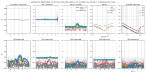
This is the resistor-free MJL1302/3281, with CFP drivers (see schematic). Source impedance 330R (mislabeled 330k on graph).
Don't look at the current gain plot, the probe is not plugged. It was not possible to measure it, because input current is too low.
Results:
The small instabilities spotted previously are still there. They look like two small spikes on both sides of gm curve. They are not crossover spikes, these occur at much higher output current.
At low bias (25mA,50mA) the deep Gm hole near zero current creates a ton of high order harmonics as the signal sweeps through the crossover. But there is a flat spot at zero current, which means a standard THD vs amplitude sweep will find distortion decreasing at low levels as the signal "fits" on that flat spot. This is an illusion: as soon as real music is applied, the whole crossover region will be visited, with a corresponding rise in distortion.
So, at low bias current, emitter resistors will most likely be a necessary evil. They don't fill the hole, but they bring down the two "wings" on both sides, which reduces changes in gm. Of course, with resistors, transistors will turn off sooner, so there will be more crossover spikes, but at low bias this is inevitable. Class D dominates the efficiency segment anyway.
At higher bias, starting from 100mA, and especially at 200mA, the Gm hole fills up. In fact, variations of 1/gm (which is the nonlinear output impedance) become small relative to the load resistor, which means the output amplitude becomes constant across the crossover. High order harmonics disappear into the noise. The change from 50mA to 100mA is quite spectacular. 200mA is essentially perfect, there is a bit of 2nd harmonic, 4th and 6th are nuked. This is excellent performance.
There is some 3rd and 5th which are constant, they do not depend on output current. They are not in the input signal which is acquired by another soundcard channel, then runs through the same algo and is displayed in grey on the graphs, to make sure we know where the measurement limit is.
In this test, the input is driven with the 3kHz tone whose distortion we're measuring, while a large 40Hz current is injected into the output. So the Vce's only move by the amplitude of the 3kHz tone, which is quite small, up to one volt. So I think these odd harmonics are simply due to Early effect and input capacitance. To test this hypothesis, I ran a test with different positive and negative power supply voltages (+10V/-20V). That tilted the odd harmonics vs output current graph strongly towards one polarity, which answered the question: it is indeed Early effect and capacitance. This is a strong selling point for a cascode output stage, in addition to the lower Vce making it easier to stabilize bias without resistors.
Attachments
-
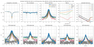 thd-F=3k-MJL1302-3281 v11 CFP Drivers Re=0 Rb=3R8 DrE=33R Rin=330k-B=25.0m,HA=4.0m,LA=2500.0m,TH.png452.8 KB · Views: 498
 -
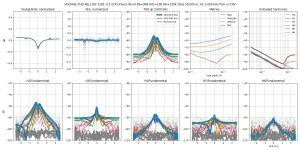 thd-F=3k-MJL1302-3281 v11 CFP Drivers Re=0 Rb=3R8 DrE=33R Rin=330k-B=50.0m,HA=4.0m,LA=2500.0m,TH.png452.7 KB · Views: 461
 -
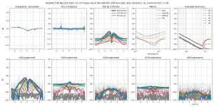 thd-F=3k-MJL1302-3281 v11 CFP Drivers Re=0 Rb=3R8 DrE=33R Rin=330k-B=100.0m,HA=4.0m,LA=2500.0m,T.png462.3 KB · Views: 460
 -
 thd-F=3k-MJL1302-3281 v11 CFP Drivers Re=0 Rb=3R8 DrE=33R Rin=330k-B=200.0m,HA=4.0m,LA=2500.0m,T.png445.4 KB · Views: 483
 -
 cfp drivers.PNG26.5 KB · Views: 520
Last edited:
Take home points:
1) At 200mA bias, the BJT output stage without resistors gives pure class A performance without the usual ridiculous dissipation. It stays in class A up to 1.5A output current!
2) Output impedance of drivers plays an important part. When output current increases, one output transistor pulls a high base current, but the other is asleep. Combined with driver output impedance, this causes a transient reduction in bias voltage (between driver emitters). This is just like setting the bias current at a lower value, and it means the transistor that is going to turn off will do so earlier than it should. Therefore, low output impedance drivers (ie, CFP) widen the range of output current where it stays in class-A. IMO this is a major advantage of CFP drivers over triples, in addition to the better thermal stability.
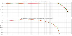
I used these low-voltage, somewhat cumbersome 2SA2039/2SC5706 drivers for two main reasons:
- Flat hFe up to 2A
- >100MHz fT from 10mA to 3A, >200MHz fT from 30mA to 2A
That last point made a huge difference on turn-off spikes. And the bandwidth that comes out of this is a lot better than what MJE15030/1 delivered... flat to 10MHz, low phase shift, and it does not depend on output current.
This topology makes a very low amount of distortion. Then it has wide bandwidth, so a ridiculous amount of feedback can be applied, to reduce it even more.
Of course MJL1302/3281 cannot do any useful amplification at 10MHz. In fact, the thing draws 1.5A from the power supply right as the network analyzer sweep hits 10MHz, most likely because of cross-conduction. But it does not matter, because in audio, there is no actual signal to amplify at that frequency. All it has to do is pretend, with low phase shift, to keep the feedback happy.
Going according to plan 😀
Attachments
lmao
I've put a ferrite bead on the power transistor bases, it got rid of the peak at 10MHz and it also got rid of all the nice bandwidth. But it's a 100 ohms bead, which is too much, so that's normal. It will do for testing. I'll order some lower impedance beads.
The mysterious spike issue was the CFP drivers having bursts of oscillation at 200 MHz or so, only at a specific point in the waveform. I spotted it on the scope. That depends very much on layout: putting a finger on it removes the oscillations. I'm not going to spend too much time on it since it may or may not occur in a proper PCB layout.
I seem to have busted the bias circuit ; perhaps the "spiderweb hanging on a pile of junk" was not the most reliable construction method 😀 It doesn't matter: it has shown that it works, so it has done its job.
Next things to try are:
1) Testing at unequal positive and negative power supply voltages resulted in an increase in distortion, which means there are similar distortion mechanisms in the top and bottom halves that cancel when power supply voltages are equal... but they do not cancel when voltages are different. As said earlier, Early effect and input capacitance are the prime suspects.
-> So, I will try bootstrapping the drivers to keep their Vce constant.
2) Cascoding the output transistors with a MOSFET, for the same reason.
Last edited:
I have a commercial amp using small caps B-E (on drivers and outputs I think), I was wondering if that was to make the input capacitance more constant and predictable..?
Hmmmmmm
I wonder... yes, maybe, or maybe let some Hf through to improve open loop phase? You could always run a simulation and compare with/without...
I'm thinking about how to separate distortion from current and distortion from voltage, to make it easier to identify the source... I think I'm gonna go back to combinations of injecting signals into the input and the output of the DUT, I'll see if I can do that tomorrow.
I have a commercial amp using small caps B-E (on drivers and outputs I think), I was wondering if that was to make the input capacitance more constant and predictable..?
Feedforward at high frequencies (to reduce crossover spikes)?
(Just a fairly outlandish complete guess!)
Guys ngspice isn't the topic, you can do that via PM.
Reichelt sells a ton of Chinese clones of mythical Japanese transistors at pretty cheap prices.
I'm going to order a few.
Anybody got a pair of the good fast SanKen's to lend me?
Send me your shipping data , I'll send you 2 pair of SAnken 2SA1386/2SC3519.
- Home
- Amplifiers
- Solid State
- Power amp OUTPUT STAGE measurements shootout