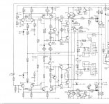
An output stage I was successfully using in the last few years, with various input and VAS stages, is here: The YAP Output Stage It was originally developed by Sansui.
Send me your shipping data , I'll send you 2 pair of SAnken 2SA1386/2SC3519.
Thanks!
An output stage I was successfully using in the last few years, with various input and VAS stages, is here: The YAP Output Stage It was originally developed by Sansui.
That was an interesting read, thanks.
The simulation with parasitics is really a must, although almost no-one does it, that's a shame. Now that 4 layer has become very cheap, we can get low impedance supply rails and decoupling caps, and it should also reduce class-AB magnetic coupling distortion since it is possible to make the current paths for positive and negative current overlap on the PCB.
I like the two transistor bias circuit (Q63/Q65 in your schematic) because it ignores Vbe tempco from the drivers, so it makes it possible to use resistor-free class AB BJTs. I was surprised that it was so easy to get it thermally stable.
Between these two schematics:

I want drivers with a low output impedance, because that keeps the bias voltage constant between power transistor bases, which widens the range of output currents where the output transistors both conduct, which gives more class A and flatter gm for less bias current. These two schematics should have roughly the same output impedance with regard to that because they're both similar, two transistors, so same current gain and open loop gain... The first is like a CFP except the driver transistor is the other way around and upside down. But the CFP has better current gain from the point of view of the VAS, while the other ignores Vbe of the driver. So it's a compromise.
In my setup it misbehaved a bit, but that's probably because I built it point to point above the pcb, which adds too much inductance. With proper layout, it should not be difficult to compensate by adding a cap between the base and collector of both transistors, if necessary.
Now...

The one on the left has 3 transistors in a loop, which is usually too much gain to be stable, so it'll need the compensation caps as you demonstrated. The one on the right uses "division of labor" to make nested loops, with the CFP drivers having their local feedback loop, and the bias control transistors having their own local compensation. I can't say which one would work better...
I have received two pairs of Thermaltrak transistors, so I will measure the transient response of the temperature sensor diode versus main transistor heating. That's the sort of stuff that should be in the datasheet, but it is not...
It's been posted before, but it is still a good link!
I'm busy modifying the software a bit. To be continued...
I'm busy modifying the software a bit. To be continued...
I've set it up to run all combinations with regard to input and output.
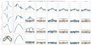
1) It injects low frequency current (LF, 40Hz, 2.5A) and high frequency current (HF, 3-6kHz, 128mA) into the output of the OPS, with the input of the OPS grounded.
The voltage that appears at the output corresponds to distortion caused purely by current through the output stage, and it ignores distortion due to voltage like Early effect, nonlinear capacitance, etc. So gm dependent distortion can't hide behind the small amount of H3 and H5 generated by these.
In this mode, current gain is not measured correctly because all the device capacitances provide some helpful base current instead of stealing it from the driving circuit.
2) It still injects LF current into the output, but now the HF goes into the input as a voltage, and that makes the OPS reproduce this HF sinewave at its output, in the presence of a LF current. So the output current is the same as above, the difference being that now transistor Vce is moving.
In this mode, current gain on the HF signal is measured correctly, including drive current lost through capacitance.
Current-dependent distortions measured at the previous step are still present, plus voltage dependent distortions.
As long as there is no clipping, and since there is no LF at the input, and the HF voltage at the input does not change along with the LF current injected at the output, distortion that depends on voltage will manifest as a constant amount of distortion added to the current-dependent distortion.
If both output transistors had mismatched voltage-dependent distortion, that "constant" amount would change depending on LF output current polarity, according to which transistor is on or off.
3) HF and LF voltages are sent into the input. Due to the opamp driving the OPS, plus headroom for the biasing current sources, drivers, etc, this limits output voltage, so current maxes out at 1A into the 8R load, it is lower lower than at the previous steps.
This is mostly to confirm the result would be the same as the previous step, to check if the setup worked:
4) same as step 3, but the load is disconnected, so we get voltage-dependent distortion only.
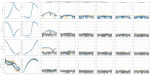
Each of these steps is a line of plots in the figure below.
X-axis is always the LF output current ; Y-axis is always in dB.
First column is the amplitude of the HF signal at the output, second is current gain, and then the harmonics of the HF signal. I got rid of the THD plots and kept only harmonics because H2 dominates THD anyway.
This one is at 100mA bias with 0R15 emitter resistors.
1) It injects low frequency current (LF, 40Hz, 2.5A) and high frequency current (HF, 3-6kHz, 128mA) into the output of the OPS, with the input of the OPS grounded.
The voltage that appears at the output corresponds to distortion caused purely by current through the output stage, and it ignores distortion due to voltage like Early effect, nonlinear capacitance, etc. So gm dependent distortion can't hide behind the small amount of H3 and H5 generated by these.
In this mode, current gain is not measured correctly because all the device capacitances provide some helpful base current instead of stealing it from the driving circuit.
2) It still injects LF current into the output, but now the HF goes into the input as a voltage, and that makes the OPS reproduce this HF sinewave at its output, in the presence of a LF current. So the output current is the same as above, the difference being that now transistor Vce is moving.
In this mode, current gain on the HF signal is measured correctly, including drive current lost through capacitance.
Current-dependent distortions measured at the previous step are still present, plus voltage dependent distortions.
As long as there is no clipping, and since there is no LF at the input, and the HF voltage at the input does not change along with the LF current injected at the output, distortion that depends on voltage will manifest as a constant amount of distortion added to the current-dependent distortion.
If both output transistors had mismatched voltage-dependent distortion, that "constant" amount would change depending on LF output current polarity, according to which transistor is on or off.
3) HF and LF voltages are sent into the input. Due to the opamp driving the OPS, plus headroom for the biasing current sources, drivers, etc, this limits output voltage, so current maxes out at 1A into the 8R load, it is lower lower than at the previous steps.
This is mostly to confirm the result would be the same as the previous step, to check if the setup worked:
4) same as step 3, but the load is disconnected, so we get voltage-dependent distortion only.
Each of these steps is a line of plots in the figure below.
X-axis is always the LF output current ; Y-axis is always in dB.
First column is the amplitude of the HF signal at the output, second is current gain, and then the harmonics of the HF signal. I got rid of the THD plots and kept only harmonics because H2 dominates THD anyway.
This one is at 100mA bias with 0R15 emitter resistors.
Attachments
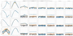
An explanation about the wiggly graphs on the first column:
Intermodulation occurs when the amplitude of signal #1 goes up and down depending on another signal. So I just plotted the amplitude of the HF tone according to output current.
btw, they're not in dB, they're just a ratio, it makes it easier to view it as percentage.
On the first line, current is injected into the output, so the output voltage corresponds only to the output impedance, which is tiny. So in comparison its variations looks large. The interesting graph is the same on the second row, which shows the variation in output voltage when the input is driven. They are very low, less than 2%.
Besides that, the current gain graph clearly shows where the turn-off spikes occur. I think that's because this is the instrumentation amplifier channel with the highest gain, so it will also pick up EMI from high di/dt events, like the turn-off spike, which is similar to a diode recovery.
-> Looks like the turn-off spike doesn't just make a mess in the output, maybe it can be picked up and amplified by the preamp too!
-> Got a phono preamp in the same box as an amp that makes turn off spikes? hmm...
Compare to the plots below, of the exact same output stage without resistors. One at 100mA, the other at 200mA.
- Crossover spikes are gone.
- All the harmonics above 3 disappear in the noise floor.
- At 200mA, H3 also disappears in the noise floor, leaving only a bit of H2.
A little bit of H3 and H5 remain on the tests where the input is driven (all except the top line). It is constant regardless of output current, so it must be voltage related.
Attachments
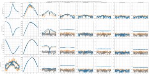
To investigate this, I use IRFP150 and IRFP9140 as bootstrapped cascodes on top of the output transistors. Their gates are 15V away from the output voltage, which gives the output transistors a constant Vce of about 10V. No cascode on the drivers yet.
Amazingly, this flying wire mess did not oscillate.
The constant low level 3rd harmonic is gone, leaving only H2 and a little bit of current dependent H3 at 100mA bias like before. It is very clean.
Amazingly, this flying wire mess did not oscillate.
The constant low level 3rd harmonic is gone, leaving only H2 and a little bit of current dependent H3 at 100mA bias like before. It is very clean.
Attachments

Last edited:
Unexpected result! With the cascode on top of the drivers too, the constant H3 that was present before came back.
Hi peufeu,
🙂
Have another look a the Carver schematics. Bob Carver is more intelligent than people give him credit for.
🙂
Have another look a the Carver schematics. Bob Carver is more intelligent than people give him credit for.
anatech> Yes, the Carver schematics were very helpful! I wasn't sure one pair of MJLs without resistors would work, or would it be enough? I was about to not even try it... But Carver uses 50mOhm resistors at quite high Vce, and only one pair, in a quite high power amp... so yeah.
I think I've found the origin of this annoying 3rd harmonic. Probably related to the setup (ie, an instrumentation amplifier that was not used got enough signal to clip and that may have introduced crosstalk into the other channels). Anyway, it's gone. If it was setup related and wasn't there to begin with, then the cascode didn't eliminate it, but I'm still happy that it works: it still brings benefits of improved SOA in the output transistors without paralleling/matching headaches, and lower dissipation which could be useful to keep bias stable without resistors. Cascode FETs are cheaper than MJLs so it's a cheaper way to increase dissipation capability too.
I've set the cascoded transistors Vce to just 6V to see how low it can go. No problems at all.
There's something wrong with the bias, because the software thinks it is 200mA, but it actually ran around 130mA. So the label on the plot is wrong. It's my DIY non-inductive resistor: after soldering and desoldering it too many times, the copper foil cracked, so its value has increased. So the plot below is at 130mA.
Anyway: I got the results I wanted:
1) At low bias currents (<50mA) emitter resistors reduce distortion, but it is a compromise, as they worsen turn-off spikes too.
2) At higher bias currents (100-200mA) no resistors is a much better option. Distortion is extremely low both in amplitude and harmonic order. Turn-off spikes are greatly reduced. Transconductance is huge. There is no gm-doubling, so a variable bias amp can be implemented.
3) Bias sensor on the transistor allows no emitter resistors without trouble (I expect ThermalTrak to work even better)
4) Cascoding the output stage and drivers works and isn't difficult ; even with air wiring and no special precautions besides 120R gate resistors on the FETs, no oscillations occured. Gates are driven through a 47µF bootstrap cap connected to the output, and biased with a 10k resistor.
So... basically this is all I wanted to do with bipolars on this setup ; testing more output stage topologies will require another PCB because I'm fed up with flying wires.
I will now compare with MOSFETs.
Attachments
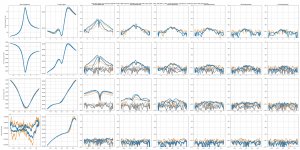
I put in the IRFP240-9240, but I left the cascodes in, at 10V Vds.
Cascodes bootstrap the input capacitance of the FETs somewhat (not completely, because their output impedance is not zero).
But the lower Vds makes input capacitance higher, which somewhat compensates... Current gain is only 20% higher with the cascode. So there is no real gain here.
Cascodes bootstrap the input capacitance of the FETs somewhat (not completely, because their output impedance is not zero).
But the lower Vds makes input capacitance higher, which somewhat compensates... Current gain is only 20% higher with the cascode. So there is no real gain here.
Hi Peufeu,
In a good AB design you can generally get H5, H7 and H9 at least lower than about 100dB, with even orders (H2 and H4) dominating the profile and a THD of about 0.01%.
Do you believe that if you can set up the outputs so that they never turn off you will improve significantly on these figures? This would improve the sound quality markedly if you could do it........
Thank you for this fascinating analysis, best I've seen here.
HD
Very informative thread, and I like your approach to prototype and test, and at the same time you have the skills to setup the measurements and come up with solutions! No PM's with job offers from high end manufacturers yet? 😉
Anyway, here I am again with another Proton schematic I found, no emitter resistors, and 'modulated rails' (I don't know the correct terminology) for drivers and single pair outputs. Seems they were on to something similar back then too. However, it seems to have the same weak link with the bias as the one I mentioned before, and Iq probably set way too low from factory to keep it from smoking.
Anyway, here I am again with another Proton schematic I found, no emitter resistors, and 'modulated rails' (I don't know the correct terminology) for drivers and single pair outputs. Seems they were on to something similar back then too. However, it seems to have the same weak link with the bias as the one I mentioned before, and Iq probably set way too low from factory to keep it from smoking.
Attachments
Last edited:
Why would "single" output devices need emitter resistors.
The rail voltage is switched high/low depending on output swing. Was a common method to limit power dissipation so you could use smaller heatsinks.
The Carver M-400 Cube used 3 rail levels back in the day. I had the misfortune to have to repair one in the 90's without a schematic. I vaguely remember the ridiculous mumbo jumbo Carver used to promote the amplifier. "Magnetic Field Amplifier"
A Paul Kemble web page - Carver Corporation M-400 MFA.
Carver M-400(a)(t) - Carver Amplifiers - Nelion Audio
Benchmark AHB2 also uses multiple fixed voltage rails with switch transistors. They then use feedforward to attenuate crossover distortion and the rail switching distortion.
Hi busaboy,
The M400 cube was the worst one Carver developed and was really a proof of concept released for production. They worked and sounded pretty awful. The point was that you could deliver that power level from a small, cool running package.
I hated the terminology that they used in advertising, but it did use a magnetic field coil, or "mag coil" as we called them. They were terrible to work on as you found out. The cost of cramming everything into a tiny space. You were not able to get a schematic because Carver Corp. recognized that a tech needed to be properly trained to repair one and normal service networks were not very good. I say this from long experience. Other brands had similar problems with service and the only defense was to force service to be performed at the factory, or an appointed depot like I was for Canada.
So you are picking on the worst Carver amplifier ever produced. The other, newer products were much better. Still, training was required to fix them properly or to service them efficiently. My advice to people today is that they shouldn't repair one of these unless they were in love with it, or needed it functional for their collection. Repair costs are normally high.
Absolutely no one enjoys working on a cube.
-Chris
Way not use low voltage Class A OPS and modulate that low voltage PS with a Class D amp like this:200W Class A amp with high efficency
I have working amp Class A and Class B to kodulate the Class A OPS PS.
The one with Class D is ready to be tested but I'm slow, hope do that soon.
Damir
I have working amp Class A and Class B to kodulate the Class A OPS PS.
The one with Class D is ready to be tested but I'm slow, hope do that soon.
Damir
So... basically this is all I wanted to do with bipolars on this setup ; testing more output stage topologies will require another PCB because I'm fed up with flying wires.
I will now compare with MOSFETs.
I hope you can perform some testing with the SAnken pairs I've send you. I'm specifically tested when driven bij a Fet driver stage and 0R22 emitter resistors with 100mA Bias.
My amp has 7 pairs of SAnken with 1530/201 drivers biased at about 120mA. Would 1 pair of Sanken bjt's driven by Fet's biased at 120/7 = +-17mA be representative?
Regards
- Home
- Amplifiers
- Solid State
- Power amp OUTPUT STAGE measurements shootout