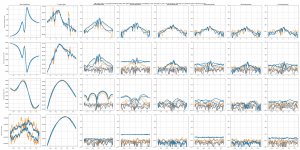
Ah, you made me remember that I compared the hyperbolic OPS with the cascode OPS!
I pulled the graphs from the non-cascode OPS, and indeed there is some 3rd and 5th due to voltage, nonlinear capacitance and Early effect, on the unloaded test (see below).
So, for the three OPS'es considered...
Common characteristics:
+ Good gm flatness starting from 100mA bias, excellent at 200mA, which means very low high order harmonics
- Not suitable at bias lower than 100mA, in this case emitter resistors will give flatter gm, but this lower bias compromises on turn-off spikes and high order harmonics
+ Wide crossover region with smooth transition in current gain between top and bottom half
+ Strong reduction in turn-off spikes due to turn-off happening at higher current
Resistor-free BJT:
- Voltage related distortion is present as odd harmonics
- Thermal stability dubious at high Vce
- Paralleling possible but needs matching
Cascode resistor-free BJT:
+ Voltage related distortion is removed due to cascode
+ Thermal stability excellent
+ Low Vce increases SOA, so paralleling is unnecessary at "living room" levels of power
Common to both OPS above:
- Requires close temperature sensor like ThermalTrak or sensor soldered on device collector, plus special circuit
- Requires very low Zout temperamental CFP drivers
Hyperbolic:
+ Voltage related distortion is removed due to feedback through control transistors
+ Good thermal stability
+ No need for CFP drivers, simple drivers are fine
+ Even wider crossover and smoother transition
+ Transistors can be paralleled with emitter resistors outside of the "constant voltage diodes", although that may increase distortion at turn-off, will have to check
Attachments
I found this HCA LTspice file by Ostripper 2009 Yamaha's Hyperbolic Conversion Amplification (HCA) Circuit
It runs, 10kHz 30Vpk 0.01%. Non-switching, 4x150mA idle with 0.22 ohm emitter R's.
But no Schottky's in emitters.
It runs, 10kHz 30Vpk 0.01%. Non-switching, 4x150mA idle with 0.22 ohm emitter R's.
But no Schottky's in emitters.
Nice catch, going to look into that...
I've run some more sims.
Previously, changing input node did not result in worse measurements because I measured at low current. At high current, input node should really be the control transistors emitters (red) and not the collector (blue).

Next, is it possible to add emitter resistors to the power transistors in order to parallel them?

It doesn't seem to change total harmonics or shape of residual. However, the bias control feedback loop has to work 10x harder with the resistors than without. This is voltage between driver bases (ie, bias voltage):

That's because, without the resistors, the bias feedback circuit makes the BJTs "emulate" their natural characteristic, which is easy and needs little correction. With resistors, the characteristic is quite different, so a lot more correction is needed.
However, the resistors are only useful when paralleling devices, so they would not be used in this scenario. Let's add 2 pairs of devices.

With 3 pairs, each with 0R33 resistors, output impedance is 3x lower, it is like having one third of the resistance value, so the bias feedback has an easier job. It only works a bit more than twice as hard, instead of 10x. So it's much better, and it looks like this design is paralleling-friendly.
Of course the diodes will still take the whole current. I used TO-220 dual Schottky STPS40M60 rated for 20A average per diode, and 220A surge for 10ms, so that should be fine. It is important to use low voltage Schottky diodes, because according to ST app note, those above 100V can exhibit standard diode recovery, which should be avoided here, because the diodes will turn off.
I've run some more sims.
Previously, changing input node did not result in worse measurements because I measured at low current. At high current, input node should really be the control transistors emitters (red) and not the collector (blue).
Next, is it possible to add emitter resistors to the power transistors in order to parallel them?
It doesn't seem to change total harmonics or shape of residual. However, the bias control feedback loop has to work 10x harder with the resistors than without. This is voltage between driver bases (ie, bias voltage):
That's because, without the resistors, the bias feedback circuit makes the BJTs "emulate" their natural characteristic, which is easy and needs little correction. With resistors, the characteristic is quite different, so a lot more correction is needed.
However, the resistors are only useful when paralleling devices, so they would not be used in this scenario. Let's add 2 pairs of devices.
With 3 pairs, each with 0R33 resistors, output impedance is 3x lower, it is like having one third of the resistance value, so the bias feedback has an easier job. It only works a bit more than twice as hard, instead of 10x. So it's much better, and it looks like this design is paralleling-friendly.
Of course the diodes will still take the whole current. I used TO-220 dual Schottky STPS40M60 rated for 20A average per diode, and 220A surge for 10ms, so that should be fine. It is important to use low voltage Schottky diodes, because according to ST app note, those above 100V can exhibit standard diode recovery, which should be avoided here, because the diodes will turn off.
It is possible to prevent the transistors from turning off by adding a resistor across both diodes, which sinks some current while one diode turns off.
This makes no change in the output THD because it is hidden by feedback, but this changes the turn-off characteristic of the BJTs, which means the bias voltage gets more distorted near crossover.
Probably not worth it. The extra current would be better invested as higher bias.
This makes no change in the output THD because it is hidden by feedback, but this changes the turn-off characteristic of the BJTs, which means the bias voltage gets more distorted near crossover.
Probably not worth it. The extra current would be better invested as higher bias.
Attachments
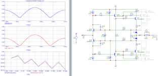
I found this HCA LTspice file by Ostripper 2009 Yamaha's Hyperbolic Conversion Amplification (HCA) Circuit
It runs, 10kHz 30Vpk 0.01%. Non-switching, 4x150mA idle with 0.22 ohm emitter R's.
But no Schottky's in emitters.
Alright. Quite interesting. I drew something very similar last week 😀
The general idea is to increase bias according to the absolute value of output current, which prevents turn-off. This "absolute value" function is computed by a class-AB output stage:

This is basically the input stage of an OTA, but it's working in class AB.
Q64 Q65 act as bias voltage generator: voltage between their emitters is input #1 which is high-ish impedance. Q66 Q67 act as followers and their emitters meet at input #2 which is a low impedance input. With the help of resistor R121, voltage between this node and GND (as an example) is turned into a current, which Q66 Q67 split in two and steer towards their collectors.
Sum of these collector currents in R113 R115 (with proper polarities) is the absolute value of input current. While it may appear impractical to have the output split in two halves, at two different places in the circuit, and with opposing polarities... it is actually a useful feature, because it means both halves can be used separately.
If the goal is to compute the absolute value of a voltage, which is the case here, both sides (left and right) are somewhat interchangeable, as long as resistor R121 is part of the circuit. This can be used to optimize the input impedance of this thing relative to source impedance, but it also inverts the output. In the Yamaha schematic, it is in the wrong direction regarding impedance, because the low impedance input faces left towards the predriver, but that's the correct direction for polarity.
Todo: check if it makes input current worse, or compensates something else and makes it cleaner.
Bias current in this small class AB stage controls how "rounded" the downward pointing tip of the absolute value curve is (last plot). It is important that it should be rounded to avoid sharp high order derivatives (ie, high harmonics).
Now that was the core of the Yamaha design, so let's get to it. Schematic presented by ostripper is unreadable but I found the original Yamaha's in the thread:


Absolute value circuit is the two rightmost dual transistors. Each has a current mirror on the output, which injects both halves of this absolute value signal into the bias controller (Q309 Q311) on the second schematic or just apply some current to resistors R229 R230 for the same effect in the first schematic. Result is the same, which is to tweak bias voltage between driver bases, and increase it in proportion with absolute value of output current.
Output current is measured through voltage between input and output of the OPS ; since output impedance is mostly determined by emitter resistors that's close enough to measuring voltage across a resistor to get current.
Let's generalize this circuit:
We can measure output current, but also its derivative. At low frequency, there are no crossover spikes and there is a lot of feedback to correct distortion. At high frequency, it's the opposite. So, as said a few pages ago, increasing bias according to absolute value of output current, or a mix of output current and its derivative, could be interesting.
So we have two possible "sources" for the correction signal: Iout, and dIout/dt.
Then this correction can be applied to the whole bias voltage, influencing both transistors... or to only one transistor, since after all, both transistors have a bias voltage, which is between their base and the input. The sum of these is the usual bias voltage, and determines bias current, but they could be handled separately.
So there are several combinations available for this circuit.
#1
Yamaha increases bias on the power transistor that has less current, while decreasing bias on the other, by sending the corresponding outputs of the absolute value circuit to the corresponding halves of the output stage or bias control circuit. When the small class AB stage in the absolute value circuit runs out of bias and one transistor turns off, then it only tweaks one transistor, which is the one with least current. This ensures a smooth transition. It will also reduce gm, which should mitigate gm-doubling. It uses a small amount of negative feedback, and it should be easy to make it stable. It increases bias on the transistor that is turning off: this transistor has lower gm and the other dominates the output, so playing with its bias while it's almost off should not increase distortion too much.
I think this circuit has a lot of potential.
It does not try explicitly to be non-switching (although it looks like it can be, with the right settings).
#2
Increase bias in both transistors, handling this as a differential signal, which would then cancel out at the output, removing distortion introduced by the process. That only works if both transistors have equal gm, which means it only happens at zero current. So the bias tweaking signal should be steered to both transistors according to need to make sure distortion cancels out. Looks complicated and annoying.
#3
Increase bias of the transistor that is on: looks suspiciously like positive feedback, with associated problems...
I will further investigate option #1. Most likely next week, because this weekend is going to be very busy.
Thanks for vindicating what I said ~10 years ago about degeneration resistors:Nice catch, going to look into that...
I've run some more sims.
Previously, changing input node did not result in worse measurements because I measured at low current. At high current, input node should really be the control transistors emitters (red) and not the collector (blue).
View attachment 974268
Next, is it possible to add emitter resistors to the power transistors in order to parallel them?
View attachment 974269
It doesn't seem to change total harmonics or shape of residual. However, the bias control feedback loop has to work 10x harder with the resistors than without. This is voltage between driver bases (ie, bias voltage):
View attachment 974270
That's because, without the resistors, the bias feedback circuit makes the BJTs "emulate" their natural characteristic, which is easy and needs little correction. With resistors, the characteristic is quite different, so a lot more correction is needed.
However, the resistors are only useful when paralleling devices, so they would not be used in this scenario. Let's add 2 pairs of devices.
View attachment 974273
With 3 pairs, each with 0R33 resistors, output impedance is 3x lower, it is like having one third of the resistance value, so the bias feedback has an easier job. It only works a bit more than twice as hard, instead of 10x. So it's much better, and it looks like this design is paralleling-friendly.
Of course the diodes will still take the whole current. I used TO-220 dual Schottky STPS40M60 rated for 20A average per diode, and 220A surge for 10ms, so that should be fine. It is important to use low voltage Schottky diodes, because according to ST app note, those above 100V can exhibit standard diode recovery, which should be avoided here, because the diodes will turn off.
Alternative buffer topologies
It is now proven beyond doubt
Thanks for vindicating what I said ~10 years ago about degeneration resistors:
Alternative buffer topologies
It is now proven beyond doubt
Yup.
I have simulated the Yamaha circuit. Well, not exactly, I have turned the input upside down, but close enough.
R121 in the middle controls the gain of the bias tweak circuit, so I stepped it.
I plotted the derivative of the transfer function (flat line = no distortion) in blue. Red is a resistor-free output stage with the same transistors. Bias is 100mA.
So basically, what the circuit does is... remove the distortion introduced by the resistors.
Attachments
Here's the file.
The function source on the bottom sets the bias current to the value defined in the text, then becomes constant during transient measurement due to the "t<=0" in the current source expression. This makes sure both circuits run at the same bias (also it can be stepped) but DC analysis will not work.
The function source on the bottom sets the bias current to the value defined in the text, then becomes constant during transient measurement due to the "t<=0" in the current source expression. This makes sure both circuits run at the same bias (also it can be stepped) but DC analysis will not work.
Attachments
Have you already received the "el cheapo" Chinese equivalents from Reichelt?
Apart from the superb analytical approach you take, I would really like to learn how far the multi device (2/3/4 pairs) OS application of super cheap power devices could be taken.
Apart from the superb analytical approach you take, I would really like to learn how far the multi device (2/3/4 pairs) OS application of super cheap power devices could be taken.
Alright!
So it looks like we'll have a shootout between a number of BJTs.
I got:
NJW0302/0281
NJL Thermaltraks
Toshiba 2SA1943 (we'll see if it is better than the ON/Fairchild version)
Toshiba 2SA1962
Unfortunately the complimentary NPN for both Toshibas were out of stock...
Bensen's Sankens did not arrive yet ;
I bought quite few cheap clones too, mostly from InChange semi.
I don't mind if it takes a while to test a pair of devices as long as it runs unattended, which means I'll use the same setup for all devices and no plugging/unplugging stuff, changing gain resistors, etc.
So I think I will run:
- turn-off spike test
- gm/hFe/thd test which shows if there is hFe droop/mismatch, it also measures input capacitance
- transient thermal impedance test, to check thermal mass and thermal resistance to heat sink
Also no way I'm gonna solder a thermal probe on each of these transistors, and I want the bias to be stable, so I think I'll just use non-inductive emitter resistors. This makes turn-off spikes worse therefore easier to measure. If I test without resistors, then the transistors with worse RthJC will heat more and bias themselves to a higher current, which would make the results useless. Another option would be to use the setup with diodes instead of emitter resistors: since voltage across the diodes controls bias current, it does not depend on the transistors, so that would make it repeatable for all devices tested.
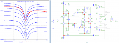
I went to do the dynamic crossover spike test on the circuit with the diodes, and then I realized the circuit on the bench was not the same as the schematic posted earlier, because I forgot to remove the 470µF capacitors that were on the board. They're C13 C14 on this schematic, which is what was tested:

Still, that gave good results, although this is not usable as-is because Q52 Q53 try to keep voltage across the diodes constant, which means bias voltage between Q60-Q61 bases needs to move, and the caps prevent that, so they will have a fight with Q52-Q53 which should result in unreasonably high current through them.
Still that thing measured remarkably well, so I'm going to investigate further.
I removed the caps, which resulted in the following circuit, minus R135 between power OPT emitters:
Hyperbolic diodes:

Without R135 this did not work at all. When one OPT turns off, the feedback loop that keeps a constant voltage between their emitters is broken, which makes Q52-Q53 go nuts: a large pulse appears at the output.
The fix is simply to make it non-switching, by adding R135. The diodes do turn off, but that should be okay since low voltage Schottky diodes do not have recovery. Power transistors stay on, with a small "alibi current" flowing through R135.
Hyperbolic diodes with constant bias:

I got good measurements with the previous schematic where the two large caps prevented Q52-Q53 from dynamically adjusting bias voltage to keep voltage across diodes constant, so I'll try this variant. Here, C6-C9 act as compensation caps on Q52 Q53, and the large value of these capacitors mean they keep the average voltage constant, but not the instantaneous voltage. Cutoff is around a few hertz, so this still ignores self-heating in the power transistors, which means there can be no thermal runaway.
Let's see who wins...
Still, that gave good results, although this is not usable as-is because Q52 Q53 try to keep voltage across the diodes constant, which means bias voltage between Q60-Q61 bases needs to move, and the caps prevent that, so they will have a fight with Q52-Q53 which should result in unreasonably high current through them.
Still that thing measured remarkably well, so I'm going to investigate further.
I removed the caps, which resulted in the following circuit, minus R135 between power OPT emitters:
Hyperbolic diodes:
Without R135 this did not work at all. When one OPT turns off, the feedback loop that keeps a constant voltage between their emitters is broken, which makes Q52-Q53 go nuts: a large pulse appears at the output.
The fix is simply to make it non-switching, by adding R135. The diodes do turn off, but that should be okay since low voltage Schottky diodes do not have recovery. Power transistors stay on, with a small "alibi current" flowing through R135.
Hyperbolic diodes with constant bias:
I got good measurements with the previous schematic where the two large caps prevented Q52-Q53 from dynamically adjusting bias voltage to keep voltage across diodes constant, so I'll try this variant. Here, C6-C9 act as compensation caps on Q52 Q53, and the large value of these capacitors mean they keep the average voltage constant, but not the instantaneous voltage. Cutoff is around a few hertz, so this still ignores self-heating in the power transistors, which means there can be no thermal runaway.
Let's see who wins...
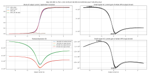
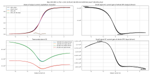
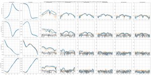
Hyperbolic diodes:
This should be compared to the resistor-free output stage with cascodes, whose results are in these two posts.
As before, the one with the diodes has a wider crossover, which is good. It is even wider, since it is non-switching... however, the transistor that is kept on does not actually participate in output current, so that measurement is a bit misleading.
At 200mA bias, the diodes give a nice gm, but it is lower than resistor-free BJTs. Transition between hFe of both halves is smooth.
Unfortunately, at the same bias current, this delivers 10dB more distortion than the resistor-free cascode output stage. I believe this is due to lower gm. This contradicts previous results with the mistake in the schematic...
There is also a gotcha: the setup counts the "alibi current" through R135 in the total bias current, which is fair since it is wasted power after all. However this current doesn't flow through the diodes, which means they are biased at a lower current than the resistor-free BJTs... and this lower bias current makes the gm dip near zero current deeper.
So I believe this could get the same performance as the resistor-free BJTs, with a bit higher bias. To confirm, I will measure the exact current in R135 and run another test with that added to the bias.
It is still better than with emitter resistors, though.
Attachments
-
 gm-Bias 100.000 m, PSU +10.0-10.0V,AC 64.000 mA 6.000 kHz,load 7.6R,HFin,LFout-MJL1302-3281 v15 .png165.8 KB · Views: 310
 -
 gm-Bias 200.000 m, PSU +10.0-10.0V,AC 64.000 mA 6.000 kHz,load 7.6R,HFin,LFout-MJL1302-3281 v15 .png165.6 KB · Views: 322
 -
 thd-Bias 100.000 m, PSU +10.0-10.0V,AC 64.000 mA 3.000 kHz,load 7.6R,HFin,LFout-MJL1302-3281 v15.jpg774.4 KB · Views: 261
 -
 thd-Bias 200.000 m, PSU +10.0-10.0V,AC 64.000 mA 3.000 kHz,load 7.6R,HFin,LFout-MJL1302-3281 v15.jpg775.2 KB · Views: 262
Last edited:
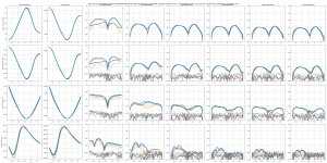
I measured 10mA through R135, so that shouldn't change the result by much.
I ran it at 220mA and 300mA bias to get a better idea of the result, and distortion did decrease, but... still not as low as the resistor-free BJTs. Notably, diodes biased at 300mA did not beat BJTs at 200mA.
I ran it at 220mA and 300mA bias to get a better idea of the result, and distortion did decrease, but... still not as low as the resistor-free BJTs. Notably, diodes biased at 300mA did not beat BJTs at 200mA.
Attachments
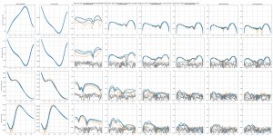
Hyperbolic diodes with constant bias:
This one is a bit more susceptible to self heating, so the actual bias is about 15% higher than what it says in the plot title.
I tested it at 100-200-300mA.
This holds AC voltage constant between OPT bases and DC voltage constant across the diodes, which means even without resistors there is no risk of thermal runaway.
However, there are now two junctions in series: the transistor's Vbe and the diode. That means gm will be half, and the gm dip near zero current will be twice as deep, but it will also be wider. Crossover is also widened, but this is not enough to compensate for the decreased transconductance, and distortion is higher.
Resistor-free BJTs still win due to higher transconductance.
Attachments
-
 thd-Bias 100.000 m, PSU +10.0-10.0V,AC 64.000 mA 3.000 kHz,load 7.6R,HFin,LFout-MJL1302-3281 v15.jpg773.8 KB · Views: 100
 -
 thd-Bias 200.000 m, PSU +10.0-10.0V,AC 64.000 mA 3.000 kHz,load 7.6R,HFin,LFout-MJL1302-3281 v15.jpg782.8 KB · Views: 109
 -
 thd-Bias 300.000 m, PSU +10.0-10.0V,AC 64.000 mA 3.000 kHz,load 7.6R,HFin,LFout-MJL1302-3281 v15.jpg798 KB · Views: 94
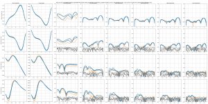
Thinking in terms of Gm is not very helpful.
S = Siemens = conductance unit = 1/ohm
Gm is 1/Zout, and the output amplitude is the result of an impedance voltage divider formed by Zout and load impedance.
Therefore, if gm varies between 5S and 10S, as with a hot resistor-free BJT, this corresponds to Zout varying between 0.1 and 0.2 ohms, which means a delta-Zout of 0.1 ohms. With a 8R load forming a voltage divider with Zout, this means output amplitude will vary by 1.25%, and distortion is proportional to this variation.
But... if gm varies between 1S and 1.11S, that looks like a much smaller harmless variation if we look at it in percentage... but that's the wrong way to look at it. It corresponds to the same delta-Zout of 0.1 ohms, because gm of 1S gives Zout=1R, and gm=1.11S gives Zout=0.9 ohms. So it would cause the same distortion as the case above.
With emitter resistors, gm is lower and looks flatter, but in terms of nonlinear output impedance, the much higher gm of BJTs without resistors is a better option.
That's why the plot on the left of the distortion graphs shows output signal amplitude, not gm.
Last edited:
- Home
- Amplifiers
- Solid State
- Power amp OUTPUT STAGE measurements shootout