With the 470µF cap, increase in H2 occurs even in the class A zone, both transistors are on, so it is not related to turn on or turn off. It also occurs when only one transistor is on, long after the other turned off. It does not happen in simulation at all.
Class A output push pull stages don't work anywhere close to constant base charge/current, only a SE class A could be approximated this way. As such, while not related to switching on/off, a large capacitor will still impede the ideal large signal base charge variations. I would think that for a Class A push pull, no cap would be the best option, but I have no direct experience with that.
While a cap helps evacuating the stored charge in the bipolar base, a too large cap will slow down the turn on of the bipolars
I had a second look at measurement results and I think what you mention is happening where the red arrows point, on the current gain graph. There are two bumps that shouldn't be there. Thanks for pointing that out.

Green circle shows high H2 over the whole range of output currents though, not just at turn-on/turn-off. So the large capacitor doesn't cause one problem, but two distinct problems.
Note I used an "insanely high" value because I wanted to know if this circuit, which is supposed to work with a large cap, would actually work with a large cap. Well, it doesn't.
I hit "preview" and I see you've already answered this one, but I don't understand what "work anywhere close to constant base charge/current" means.
Open loop bandwidth is not a relevant metric, it is the unity loop gain frequency that matters.
Yeah, I used the wrong term.
Increasing the compensation order is the only way to increase the available loop gain at HF, otherwise increasing the unity loop gain frequency always comes to a stability margin price, since audio amplifiers are minimum phase systems and, as a result, the loop gain and and loop gain phase are not independent variables.
Then why can we buy opamps with GHz ULGF?
That's why you'll see very few commercial amplifiers using even a two pole compensation schema, they prefer to play safe rather than risking costly repairs under warranty. For the same reasons, unity loop gain frequencies over 1MHz in commercial amps are as rare as hen's teeth.
Yes.
Commercial has much stricter requirements. Someone will use ultra-high capacitance audiophile cable and the amp should be idiot-proof. And someone will pick a 1µF film cap, think "oh that definitely looks like a loudspeaker", and plug it into the output.
My requirements are: it should be stable with my speakers. That's much simpler. I will still add a protection circuit, though.

Then why can we buy opamps with GHz ULGF?
Those op amps are built with devices having a Ft of 10-20GHz or even more, not with Ft=30MHz power transistors.
Class A output push pull stages don't work anywhere close to constant base charge/current, only a SE class A could be approximated this way. As such, while not related to switching on/off, a large capacitor will still impede the ideal large signal base charge variations.
What did you mean by "Class A output push pull stages don't work anywhere close to constant base charge/current"?
I'm having trouble with the word "constant", considering it's an AC signal.
I would think that for a Class A push pull, no cap would be the best option, but I have no direct experience with that.
Yes, I think this is the case too. Here are the emitter currents of a push pull stage with (red) and without resistors (blue), in simulation:

I used a log vertical scale to make the low currents easier to see. Without resistors it stays in class A up to a much higher current, which means the transistor that will turn off does so at a lower di/dt, so it has more time to get rid of stored charge. Both factors mean a softer turn-off. On top of that, without emitter resistors, transconductance of the transistor that is on at this moment is not limited to 1/Re but much higher instead. The one that is turning off has very low transconductance, so if it tries to make a mess at turn-off, the other is better able to controls the output... unless the transistor that is turning off couples with the other's base through the "speedup cap" and forces it to output the wrong signal, which seems to be another gotcha with this cap.
In fact, since I replaced the slow drivers with faster ones and got rid of the emitter resistors, I'm not seeing any turn-off spikes at all with the MJL's.
What I am seeing is: when going through the middle of the crossover, gm gets lower, so the base voltage has to swing faster to compensate, and due to base capacitance this requires an increase in drive current at this point of the waveform. Basically, the Cbe*dVbe/dt part of Ib becomes significant relative to the Ic/hFe part of Ib. This also looks like a spike, but it's not the same mechanism.
Those op amps are built with devices having a Ft of 10-20GHz or even more, not with Ft=30MHz power transistors.
Great! So we agree then 😀
It was clear from the beginning that the feedforward ULGF booster stage would not use the big slow output devices, it must be smaller faster devices with high fT at the current they're biased at. That's why I bought a tube of those.
Last edited:
I think the best solution will be to get rid of the cap entirely, which makes it possible to change the bias voltage at any time without having to charge and discharge the cap.
Then use a circuit to boost bias only when needed, when dIout/dt gets high enough. IMO this is much better than the usual non-switching designs, which have to react through feedback when the transistor is about to turn off.
When abs(dIout/dt) goes above a certain threshold while output current is going towards zero, it means there will be a mess at the next crossover. So it is predictive, it provides information before the problem occurs, which means there is enough time to increase bias current smoothly so when it gets to the problem point in the waveform... the problem doesn't occur at all.
Then why can we buy opamps with GHz ULGF?
There's a world beyond audio... opamps are used for all sorts of thing up well into RF realms. Distortion performance will be shocking of course, not an issue for RF (or even video opamps). Current feedback is normal as circuit impedances have to be in the 100's of ohms range.
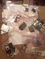
Alright. I will test this heap of transistors this afternoon, so please review the procedure, because I don't want to do it twice.
1) turn-off spike test using the oscilloscope
I'm not sure I should use the drivers, because that introduces an extra variable.
For biasing, I can't use the Vbe multiplier attached to the heat sink, because heating up the heat sink is too slow. I can't use the thermal probe on the collector either because it takes too long to solder. And I can't use the thermal probe transistor on top of the devices because it is not reproducible, results differ depending on where it is on the transistor package. So I think I will just use constant voltage bias, which the software adjusts while measuring current in the transistors at the beginning of the test. So they will all start with the same bias current.
I will use low Vce like 10V and 0R33 emitter resistors to keep bias stable when they heat up. It may seem counter-intuitive to reintroduce emitter resistors but... without them, the transistors with worst thermals would heat more, get a lot higher bias, and thus "cheat" at the turn-off spike test. Besides, emitter resistors make turn-off spikes worse, easier to measure, and less dependent on bias. I will assume that as long as all transistors use the same setup, it will be possible to compare them, and the results should translate well enough to a resistor-free output stage.
The same test also gives information about hFe matching and droop, because it also measures base current.
Therefore, TODO: I will also add a step to the turn-off spike test script to set bias to zero, with something like 0.7V between the bases instead of the usual "a bit more than 1.2V" that biases both transistors into conduction. This is to get something like a 0.5 volts "pure class C" crossover zone, where both transistors are off, so the turn-on and turn-off of each can both be observed as separate events, without the transistors interacting together as they usually do when biased in class AB.
I need to change the setup between the turn-off spike test and the distortion test, and if I do that for each transistor, considering how many there are, I will inevitably forget to do one of the changes at some point. So I think I will do all the transistors without changing the setup.
2) Transistors that pass this one will then get the distortion test.
Yes, I was highlighting the fact that syn08's assertion:
...is dependent on an implicit "while keeping output devices the same and routing all output signal through them".
With a little bit of feedforward through faster devices that don't handle the main output current, this implicit assumption is contradicted, and thus there is no problem.
1) turn-off spike test using the oscilloscope
I'm not sure I should use the drivers, because that introduces an extra variable.
For biasing, I can't use the Vbe multiplier attached to the heat sink, because heating up the heat sink is too slow. I can't use the thermal probe on the collector either because it takes too long to solder. And I can't use the thermal probe transistor on top of the devices because it is not reproducible, results differ depending on where it is on the transistor package. So I think I will just use constant voltage bias, which the software adjusts while measuring current in the transistors at the beginning of the test. So they will all start with the same bias current.
I will use low Vce like 10V and 0R33 emitter resistors to keep bias stable when they heat up. It may seem counter-intuitive to reintroduce emitter resistors but... without them, the transistors with worst thermals would heat more, get a lot higher bias, and thus "cheat" at the turn-off spike test. Besides, emitter resistors make turn-off spikes worse, easier to measure, and less dependent on bias. I will assume that as long as all transistors use the same setup, it will be possible to compare them, and the results should translate well enough to a resistor-free output stage.
The same test also gives information about hFe matching and droop, because it also measures base current.
Therefore, TODO: I will also add a step to the turn-off spike test script to set bias to zero, with something like 0.7V between the bases instead of the usual "a bit more than 1.2V" that biases both transistors into conduction. This is to get something like a 0.5 volts "pure class C" crossover zone, where both transistors are off, so the turn-on and turn-off of each can both be observed as separate events, without the transistors interacting together as they usually do when biased in class AB.
I need to change the setup between the turn-off spike test and the distortion test, and if I do that for each transistor, considering how many there are, I will inevitably forget to do one of the changes at some point. So I think I will do all the transistors without changing the setup.
2) Transistors that pass this one will then get the distortion test.
There's a world beyond audio... opamps are used for all sorts of thing up well into RF realms. Distortion performance will be shocking of course, not an issue for RF (or even video opamps). Current feedback is normal as circuit impedances have to be in the 100's of ohms range.
Yes, I was highlighting the fact that syn08's assertion:
Increasing the compensation order is the only way to increase the available loop gain at HF, otherwise increasing the unity loop gain frequency always comes to a stability margin price
...is dependent on an implicit "while keeping output devices the same and routing all output signal through them".
With a little bit of feedforward through faster devices that don't handle the main output current, this implicit assumption is contradicted, and thus there is no problem.
If you could put 80dB negative feedback around output device at 10KHz, you don't even need bias to achieve reasonable THD figure. (talking about 0.01% THD range @ 1W)
I wish I could have 1G ULGF.
I wish I could have 1G ULGF.
Last edited:
" use constant voltage bias" - use constant current bias?
Constant voltage bias between power transistor bases.
But I won't be using that...
I've put the emitter resistors back in, which brought back the ugly switching spikes. Then I discovered the bias circuit that worked very well without emitter resistors throws a spike of its own when it gets kicked too hard by the transistor base currents at switching.
So I rewired it to only compensate for the driver's slow Vbe drift due to self heating, which means better bias stability, but it is no longer attempting to keep voltage constant between power transistor bases. The mod is simply increasing the compensation cap to a ridiculous value of 470µF. Above about 1Hz, it keeps voltage between driver bases constant, just like a Vbe multiplier would, but at DC it adjusts it to compensate for drivers Vbe drift.
This seems to work nicely, and it includes the drivers in the equation. Might add an additional variable, but... can't use these transistors without drivers in an amp...
With 0R33 emitter resistors, I will test with the following bias currents:
50mA 100mA and 0mA
Should I add 25mA?
50mA 100mA and 0mA
Should I add 25mA?
If you could put 80dB negative feedback around output device at 10KHz, you don't even need bias to achieve reasonable THD figure. (talking about 0.01% THD range @ 1W)
I wish I could have 1G ULGF.
2MHz is 2 decades from 20kHz. If you use 2 pole compensation you get 40dB/decade open loop gain falloff, here's your 80dB. You need a bit of frequency margin to allow the phase to transition from -180 to something more civilized before it reaches unity gain, so ULGF won't be 2MHz, it will be higher, but it won't have to be 1GHz either...
I haven't ever been able to get more than 70dB of excess gain at 20 kHz, and that was a twitchy beast whose recovery from slewing (and recovery from clipping) was, let's just say, abnormally entertaining.
Also entertainingly abnormal.
Also entertainingly abnormal.
Yeah, it's gonna be entertaining!
Can you share the schematics?
Meanwhile...
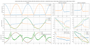
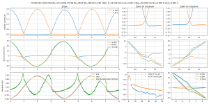
I re-ran MJL1302 and MJL3281 through the spike test for reference. This is 50mA bias, 2.5A current.
Much uglier with the emitter resistors than without them...
Can you share the schematics?
Meanwhile...
I re-ran MJL1302 and MJL3281 through the spike test for reference. This is 50mA bias, 2.5A current.
Much uglier with the emitter resistors than without them...
Attachments
-
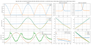 scope-Bias=50.000 mA Iout=2.560 A F=12.000 kHz--MJL1302-3281 v20 A2039-C5706 Re=0R33 Rb=3R8 DrE=.png262.1 KB · Views: 317
 -
 scope-Bias=50.000 mA Iout=2.560 A F=24.000 kHz--MJL1302-3281 v20 A2039-C5706 Re=0R33 Rb=3R8 DrE=.png277.8 KB · Views: 321
 -
 scope-Bias=50.000 mA Iout=2.560 A F=48.000 kHz--MJL1302-3281 v20 A2039-C5706 Re=0R33 Rb=3R8 DrE=.png289 KB · Views: 331
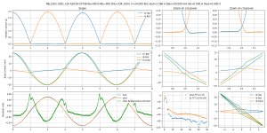
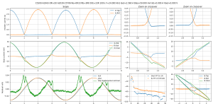
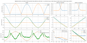
And this is the previously tested 2SC5200/2SA1943 from ON/Fairchild. I'm running them again to check the result is the same as before.
It is the same: they seem to take much longer to turn off, and when it finally happens, there is a vertical cliff on the THD residue (bottom plot).
FAIL
It is the same: they seem to take much longer to turn off, and when it finally happens, there is a vertical cliff on the THD residue (bottom plot).
FAIL
Attachments
-
 scope-Bias=50.000 mA Iout=2.560 A F=48.000 kHz--C5200-A1943-ON v20 A2039-C5706 Re=0R33 Rb=3R8 Dr.png292.2 KB · Views: 317
 -
 scope-Bias=50.000 mA Iout=2.560 A F=24.000 kHz--C5200-A1943-ON v20 A2039-C5706 Re=0R33 Rb=3R8 Dr.png273.4 KB · Views: 309
 -
 scope-Bias=50.000 mA Iout=2.560 A F=12.000 kHz--C5200-A1943-ON v20 A2039-C5706 Re=0R33 Rb=3R8 Dr.png262.8 KB · Views: 140
Last edited:
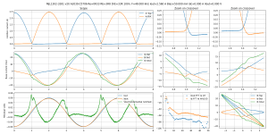
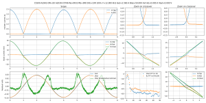
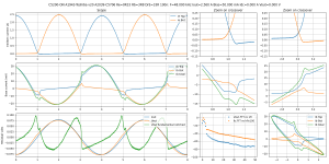
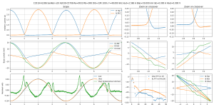
Unfortunately, Toshiba 2SC5200 was out of stock, but I got a Toshiba 2SA1943.
I test it paired with OnSemi C5200.
It is still a bit worse than the MJLs, but much better than the ON version.
So, if you like A1943/C5200, Toshiba looks like a better choice for this test.
A1943 from ON also had some hFe droop issues at high current, so I will keep these for the distortion test.
I hope I can find a Toshiba C5200...
Attachments
-
 scope-Bias=50.000 mA Iout=2.560 A F=12.000 kHz--C5200-ON A1943-Toshiba v20 A2039-C5706 Re=0R33 R.png261.9 KB · Views: 108
 -
 scope-Bias=50.000 mA Iout=2.560 A F=24.000 kHz--C5200-ON A1943-Toshiba v20 A2039-C5706 Re=0R33 R.png277 KB · Views: 109
 -
 scope-Bias=50.000 mA Iout=2.560 A F=48.000 kHz--C5200-ON A1943-Toshiba v20 A2039-C5706 Re=0R33 R.png296.4 KB · Views: 132
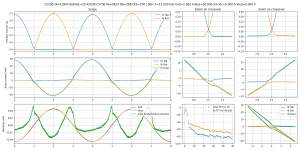
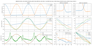
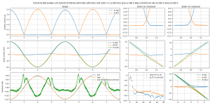
NJW0302/NJW0281 from ON are the smaller cheaper versions of the big MJL transistors.
They behave in a very similar manner, turn-off is even a little bit cleaner.
Being smaller, they self-heated to about 120mA on the 50mA setting, whereas the big ones only self-heated to 75mA. That doesn't change the results much, because with resistors, you always get the switching spikes no matter what the bias is 😀
Result: WIN
Attachments
-
 scope-Bias=50.000 mA Iout=2.560 A F=48.000 kHz--NJW0302-0281 v20 A2039-C5706 Re=0R33 Rb=3R8 DrE=.png286.1 KB · Views: 146
 -
 scope-Bias=50.000 mA Iout=2.560 A F=24.000 kHz--NJW0302-0281 v20 A2039-C5706 Re=0R33 Rb=3R8 DrE=.png278.9 KB · Views: 127
 -
 scope-Bias=50.000 mA Iout=2.560 A F=12.000 kHz--NJW0302-0281 v20 A2039-C5706 Re=0R33 Rb=3R8 DrE=.png263.4 KB · Views: 113
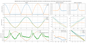
SanKen C3519-A1386 from Bensen 😀
They are very similar to ON NJW0302/0281.
ON's have a few dB less harmonics on the FFT, but the SanKen's have better hFe matching, although that could be a lucky pair.
Result: WIN
They are very similar to ON NJW0302/0281.
ON's have a few dB less harmonics on the FFT, but the SanKen's have better hFe matching, although that could be a lucky pair.
Result: WIN
Attachments
-
 scope-Bias=50.000 mA Iout=2.560 A F=48.000 kHz--C3519-A1386 SanKen v20 A2039-C5706 Re=0R33 Rb=3R.png287.6 KB · Views: 141
 -
 scope-Bias=50.000 mA Iout=2.560 A F=24.000 kHz--C3519-A1386 SanKen v20 A2039-C5706 Re=0R33 Rb=3R.png276.2 KB · Views: 132
 -
 scope-Bias=50.000 mA Iout=2.560 A F=12.000 kHz--C3519-A1386 SanKen v20 A2039-C5706 Re=0R33 Rb=3R.png267.7 KB · Views: 125
- Home
- Amplifiers
- Solid State
- Power amp OUTPUT STAGE measurements shootout