Looks like an absolutely practical quantum tweak 😀
I did not include it in the plot due to its low dissipation and tiny package, but if you allow medium power transistors, A2039/C5706 take the crown for fast switching and low charge storage...
I did not include it in the plot due to its low dissipation and tiny package, but if you allow medium power transistors, A2039/C5706 take the crown for fast switching and low charge storage...
Attachments

Gold doping was/is extensively used in TTL and other bipolar logic families and RF transistors to reduce storage time - Au dopant provides energy levels in the middle of the bandgap that make carrier-recombination far more rapid (such things are called deep traps in semiconductor physics). Downside is the raw analog performance is compromised (gain will be low for one thing, and leakage currents high, since there is much more recombination in the base).
The 2N2369A has a storage time measured in ns, not µs, and its gain is only guaranteed above 20 for many currents - this confirms its designed for logic use and is likely gold-doped.
BTW a gold-doped output transistor would probably have the gain of a 2N3055!! You could just use a gold doped RF power transistor for an output device if you want - though the voltage rating will be rather low, and linearity is probably awful (not an issue for many RF applications where the harmonics are simply filtered out).
Perhaps I could try some of the power BJTs specifically designed for switching... although they are becoming extinct these days.
RF transistors are too expensive, exotic, unrealistic.
But, to be honest, the two winners are fast enough. The key is to remove the emitter resistors and use a generous amount of bias current like 100-200mA. Without resistors they have a much larger class-A region over which they have plenty of time to turn off. Also, the transistors bootstrap each other's Cbe much more efficiently: from what I measured, when the resistors are removed, off-state Cbe appears 3x smaller than with 0R33.
Attachments
@peufeu
Could you consider analyzing this CPLHF output stage I have used in my last two projects? Idea is to use two well-matched same type MOSFETs in push-pull arrangement for good cancelation of gm nonlinearity. I am using it with high bias current enabling continuous class A operation. However, this arrangement seems to provide smooth transition to class AB operation, so it might be interesting also in the context of this thread.
Its important feature is that it ensures ΔVgs1 = -ΔVgs2, at least at low frequencies, both for excitation from input or output side. Source resistors are omitted for closer fit to square low (although it could be different story when used with lower bias current).
In my latest implementation Q1=IRF9610, Q2=Q3=IRFP240, Rgs=270R, I1~32mA (adjustable and thermally compensated for Vgs(t) of MOSFETs).
I think it's nice for class A: it will have symmetrical gm and a deep distortion null near zero current if the devices match, which should be the case if they're the same. That's a better "smooth first watt" design than push pull FETs which have a "tilted" gm since the N-channel and P-channel don't match, and certainly much better than anything with emitter resistors, since those have a dirty first watt. But, well, it's class A, so it's gonna dissipate a lot.
There's going to be some sticky clipping on the negative rail because the lower FET only has a resistor to turn it off, so if clipping occurs often perhaps a pre-clipping circuit would be a good idea, like a diode to clamp the input voltage.
I did not test any common source designs because they don't fit my high-ULGF plans. This is because of the 2nd pole introduced by the common source device which introduces some extra phase shift. In the case of a design like this one, it has one pole when the top FET conducts, two poles when the bottom one does, and when both conduct the phase shift is between the two values depending on which FET has higher current and gm.
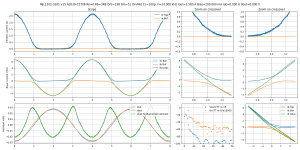
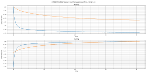
Let's test the ThermalTrak diode temperature sensor.
The transistor is heated by 1.2A at Vce=10V, ie 12W. The diode is biased at 1.5mA. Plots are scaled to a power of 1W, to get a result in millivolts of Vbe (or diode) per dissipated watt.
First plot for comparison is a configuration tested previously: MJL3281 with a MMBT3904 soldered on the collector lead as close as possible to the package.
Second plot is the NJL3281 with ThermalTrak diode.
MJL3281 (without diode) and NJL3281 (with diode) have almost identical thermal impedance, which was expected.
But... the diode reacts about as fast as the DIY option with the MMBT3904, not faster! Kinda disappointing. Well, at least it's isolated, there's always that.
The diode measures the temperature of the leadframe and not the chip. When it dissipates power, the chip gets hotter than the leadframe, and the sensor does not measure this. However, on cooling, the chip quickly returns to the leadframe temperature. At this point, when heating power is no longer applied, both the transistor and the diode act as thermal sensors on the same leadframe, so they track quite well.
So, an error is introduced in the temperature measurement: dissipated power multiplied by thermal resistance junction to leadframe.
Suppose the device is dissipating power P ; it has thermal resistance junction to leadframe R1 and thermal resistance leadframe to heatsink R2. Then, the chip is P*(R1+R2) °C hotter than the heatsink. But the thermal sensor, which is on the leadframe, is only P*R2 °C hotter than the heatsink... or P*R1 cooler than the transistor.
It looks like the diode tempco matches the transistor, perhaps a bit on the low side (in absolute value). That depends on current through the diode though. Anyway, if they both have the same tempco, It looks like R2 is 72% of the total thermal resistance, and R1 is the rest. With a worse quality silpad, it would be different. So, the sensor allows to compensate up to 72% of the transistor's heating, with a delay of a few seconds. That's not bad, still much better than a Vbe multiplier on the heat sink.
Some gain could be applied to get a better compensation, that would work when the transistor dissipates constant power. But when it cools down, it would overcompensate and underbias.
Perhaps the complaints about the diode tempco not matching the transistor's are actually due to a design choice by ON to avoid underbias on cooldown.
The irony of the situation is the MMBT3904 bodge behaves a bit like this: it has slightly more gain (perhaps more tempco than the diode) so it tracks a bit better when heating, and a bit worse when cooling... and it had excellent bias regulation without underbias.
That shows it is possible to get away with some gain, because after a high dissipation passage, the BJTs will not go back to zero power, but to the preset bias current. So they will always be hotter than the diode.
Anyway. I hoped it would be faster, but it is about as good as the MMBT3904 bodge. That one worked wonderfully with a Vce of 10V and no emitter resistors, at quite high bias currents, but at higher Vce it was less stable of course.
So, I'll either need a cascode, or some circuit that computes instantaneous junction temperature
Attachments

From your ThermalTrak plots, the gap you see is not actually delay. You could change the bias current of the thermal diode to get them align.
The actural delay is very small. I believe is less than 1 second.
The actural delay is very small. I believe is less than 1 second.
What current do you recommend?
https://www.ti.com/lit/pdf/sboa277
In your case, use less current for the thermal diode will make the curve of the diode more deep.
A pure delay will create a phase shift without change the amplitude throughout the frequency. I don't think it is the case here.
Here is more like 1 pole system with big time constant (because of the thermal mass). Just as your mentioned, you can add some gain to get more accurate control and it should remain stable. Just don't put too much gain.
Here is more like 1 pole system with big time constant (because of the thermal mass). Just as your mentioned, you can add some gain to get more accurate control and it should remain stable. Just don't put too much gain.
Last edited:
I had forgotten to divide by dissipated power, so the plots in the previous post show Vbe drift for a power of about 13.5W (10V/7.5R load resistor). This is fixed, next plots will be scaled to mV Vbe per W.
If you look at the beginning of the waveform, it is easier to see the "delay". You can call it "high order lowpass filter" if you want, that would be more accurate. Vbe reacts very quickly ; the diode has a strong lowpass effect which is normal because of the thermal mass of the leadframe... I guess the thick leadframe is a factor that helps a lot for the huge SOA of this transistor so it's nice to have it.
It should be possible to make it quicker with some gain and a filter.
Attachments
After doing a few sims using this recorded data, it looks like a cascode output stage with 10V Vce will be thermally stable even at very high bias current. This is not just due to low Vce limiting dissipation at idle: dissipation is much lower even when output power is high, which limits transient heating of the transistor chip and prevents massive overbias/runaway right after a "hot" high power passage.
It is the combination of both factors that makes it unstable without the cascode.
With the cascode, dissipation at high output power is proportional to current, because Vce is mostly constant, and it is independent of load impedance angle and phase shift between current and voltage. But without the cascode, dissipation is much higher, and dependent on current/voltage phase shift, as usual.
After a short "hot" passage the transistor chips are hot, so they have lower Vbe, but the diode sensors haven't caught up yet. So as it returns to idle, it's just like having a much higher bias setting for a short time until it cools down... With the cascodes, it works. Without them, the transistors heat a lot more at high power, and the higher Vce makes them a lot susceptible to runaway, because the increase in bias current due to each 2.5mV/°C on Vbe causes more watts of idle power, and more heating. And it runs away.
So... cascodes.
Since that makes the output devices SOA ridiculously high, it should be possible to get away with one pair for a "living room" amp.
This brings 2 questions:
- Important for stability: what happens to frequency response and phase at high current and low Vce? The SanKens seem to hold fT better at high current, so I should check that.
- If I stick a thermal sensor on the collector lead of the SanKens, will it work too?
Last edited:
I guess your goal is to remove Re entirely from the output devices. Without Re, thermal compensation is hard to design.
There is another approach. Since it is hard to get it right, just avoid it entirely.
Use 0 bias output stage (no thermal runaway issue even with 0 Re), and complement it with a small current class A (50mA to 100mA is good enough to coupe the dead zone). Quad 405 is an example.
There is another approach. Since it is hard to get it right, just avoid it entirely.
Use 0 bias output stage (no thermal runaway issue even with 0 Re), and complement it with a small current class A (50mA to 100mA is good enough to coupe the dead zone). Quad 405 is an example.
Last edited:
I measured NJL1302 on the same setup.
I guess the PNP chip is larger than the NPN: it has more thermal mass, which is good. And the diode captures less of the chip heating, which is bad. I guess more of the heat goes "vertical" into the heatsink and less goes "lateral" to heat the leadframe the diode sits on.
But besides that, pretty much the same. So.. no problem, at 10V Vce, it will work just as well as the bias stabilization circuit that used MMBT3904s on the collector leads, and that worked very nicely.
It's cheaper to dissipate heat in FET cascodes than to use 2 pairs of MJL/NJL anyway.
> Use 0 bias output stage (no thermal runaway issue even with 0 Re), and complement it with a small current class A (50mA to 100mA is good enough to coupe the dead zone). Quad 405 is an example.
Yeah but that doesn't work
Attachments
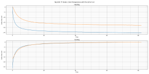
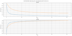
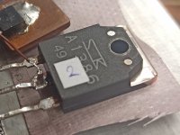
This is SanKen C3519/A1386. Thermal sensor is a MicroMELF diode soldered to the collector lead. This is much easier to do than soldering a MMBT3904 (fiddly) or a SMD LED (breaks all the time).
It still works much better than the Vbe multiplier transistor on the heatsink, but compared to ThermalTrak, it is slower and captures less of the junction temperature.
But... I just realized I soldered a 0.1" header on top of the diode, which is quite large compared to it. So I will try again with some very thin wrapping wire.
Note the thermal resistance of the Sankens is very good, 0.7°C/W junction to heat sink for the PNP and 1.16°C/W for the NPN ; difference could be due to chip size or one screw being tighter than the other.
Attachments

Last edited:
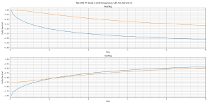
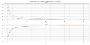
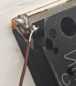
The 0.1" header that was on top of the diode has been replaced with thin wrapping wire. This steals less heat from the diode, and it tracks the temperature of the collector lead much better!
For the PNP, it is almost perfect. Even better than the ThermalTrak! For the NPN, it is comparable to ThermalTrak, but a bit slower (without electrical isolation however).
This difference is probably due to the larger PNP chip having its edge closer to the collector lead, so it transfers heat better to the sensor.
Attachments
Last edited:
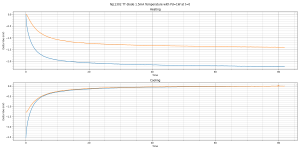
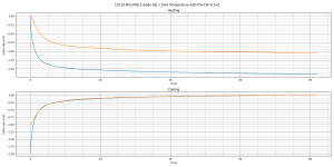
Here are pics of where the sensor diode is soldered.
I tried on the corner of the TO3P tab, and for the NPN, it worked a lot better than on the collector lead! It still doesn't capture the full temperature when heating, but when cooling, it works much better than on the collector lead. There is no lag on cooling, which means there is no risk of underbias... and a bit of gain could be applied to capture more of the heating.
So that exposed copper tab is a nice feature of the TO3P package.
Attachments
Regarding SOA, both MJLs and SanKen A1386-C3519 can do 10V Vce - 10A Ic . Datasheets specify good hFe up to 10A too. This means for realistic living room power levels, one pair will be enough.
This is my preferred option because it has the lowest capacitance, and while many pairs in parallel reduce THD when using emitter resistors, previous measurements showed that without resistors, at constant total bias, one pair was either the same or slightly better than two. That's basically the opposite of what happens with emitter resistors, quite remarkable...
So, without resistors, there is no benefit to several pairs besides power handling (at the cost of increased capacitance and matching headaches) ; and cascodes solve the power handling problem while allowing to get rid of the resistors.
Now that I have decided on cascode + 1 pair without emitter resistors, let's check the frequency response at low Vce and high current.

On the left is a standard EF2 ; the Vbe multiplier is on the board but not in the sim. On the right is the topology I used earlier, which cancels driver Vbe drift. Let's call it "CVB" or Constant Voltage between Bases of the power devices. It yielded better distortion performance, similar to CFP drivers, but without the tendency to misbehave.
Spice predicts very similar frequency response for both.

However, the CVB topology with MJL transistors and SanKen's isn't looking so good with real components...


...but EF2 is absolutely fine and delivers the expected frequency response.


I have no idea what happened here. It could simply be that the CBV bias controller, which is air-wired, broke yet again. I will postpone that to when I make a real PCB for it, and focus only on the EF2 measurement.
A more interesting data point is that at low Vce (5V) and high current (4.5A) the SanKens hold their high frequency performance much better than the MJLs. fT information from the datasheets confirms this:


So, the SanKens would offer increased phase margin and higher ULGF. That's nice.
This is my preferred option because it has the lowest capacitance, and while many pairs in parallel reduce THD when using emitter resistors, previous measurements showed that without resistors, at constant total bias, one pair was either the same or slightly better than two. That's basically the opposite of what happens with emitter resistors, quite remarkable...
So, without resistors, there is no benefit to several pairs besides power handling (at the cost of increased capacitance and matching headaches) ; and cascodes solve the power handling problem while allowing to get rid of the resistors.
Now that I have decided on cascode + 1 pair without emitter resistors, let's check the frequency response at low Vce and high current.
On the left is a standard EF2 ; the Vbe multiplier is on the board but not in the sim. On the right is the topology I used earlier, which cancels driver Vbe drift. Let's call it "CVB" or Constant Voltage between Bases of the power devices. It yielded better distortion performance, similar to CFP drivers, but without the tendency to misbehave.
Spice predicts very similar frequency response for both.
However, the CVB topology with MJL transistors and SanKen's isn't looking so good with real components...
...but EF2 is absolutely fine and delivers the expected frequency response.
I have no idea what happened here. It could simply be that the CBV bias controller, which is air-wired, broke yet again. I will postpone that to when I make a real PCB for it, and focus only on the EF2 measurement.
A more interesting data point is that at low Vce (5V) and high current (4.5A) the SanKens hold their high frequency performance much better than the MJLs. fT information from the datasheets confirms this:
So, the SanKens would offer increased phase margin and higher ULGF. That's nice.
Semiconductor supply chains in the automotive industry are no longer operational, leading to a global shortage of chips, Bosch board member Harald Kroeger cited business television channel CNBC on Aug.24.
He explained that some of these semiconductors take six months to produce. And the system where the company receives an order every two weeks is no longer working. There is a need to increase semiconductor inventories in parts of the supply chain, Kroger said. He called on semiconductor suppliers to change the approach to the supply of electronic components, which are used in many areas: automotive, computer, household appliances and others.
A Bosch manager noted that supply chains were disrupted in the past year. Then, along with the growth in demand, during the pandemic, several key semiconductor factories closed.
In addition, a winter storm in February 2021 in Texas resulted in a power outage at NXP Semiconductors, a major supplier of chips for cars and mobile phones. In March of this year, a fire broke out at a semiconductor manufacturing plant in Japan, owned by Renesas.
Most of the semiconductors are produced in Asia. If you build more factories around the world, you can accelerate deliveries, cited the opinion of the managing director of the Silicon Saxony technology network, Frank Bosenberg, in a CNBC material. He noted that only half of the semiconductors it needs are produced in Europe.
Bosch predicted an increase in demand for electronic components and built a new € 1.1 billion semiconductor plant in Dresden. It was recently opened in June 2021.
Other major players in the field of microcircuits - Intel and TSMC - also thought about building new factories. They plan to open chip factories in the next few years, CNBC reported.
The plant will produce new silicon carbide (SiC) chips developed by Bosch, or silicon carbide semiconductors.
I second Mike
Yes, this is excellent, keep up the great work Pierre.
This work is answering some questions I've had for a long time.
Thank You.
Yes, this is excellent, keep up the great work Pierre.
- Home
- Amplifiers
- Solid State
- Power amp OUTPUT STAGE measurements shootout