I should have run a simulation 😀
Spice confirms: every nH is too much, the ideal would be below 10nH. This means layout is critical, and the usual single layer amplifier board will degrade crossover performance. Will the slow TIPs be more user-friendly in this department? Spice says no...
MOSFETs don't care.
Spice confirms: every nH is too much, the ideal would be below 10nH. This means layout is critical, and the usual single layer amplifier board will degrade crossover performance. Will the slow TIPs be more user-friendly in this department? Spice says no...
MOSFETs don't care.
Last edited:
I did a simulation of four bias currents (1 mA, 7 mA, 20 mA, and 50 mA) for the emitter currents.
For 20 Vpp output, the distortion of the 2nd harmonic at 20 kHz is
1 mA: -46 dB
7 mA: -47 dB
20 mA: -48 dB
50 mA: -47 dB
However, if you examine the higher harmonics, there is significant less distortion at the odd higher harmonics because the cross-over distortion is less.
I think the even harmonic distortion is due to the asymmetry in the gain of the NPN and PNP, which in the model NPN BF=260 in the model and PNP BF=120. These are the OnSemi spice models used.
I saw an increase in distortion with emitter resistor inductances as high at 1000 nH, but emitter resistor inductances on the order of 100 nH seems to have little effect.
A ZIP file with the Qucs-S schematics, ngspice simulation, and the results is attached.
Attachments
Last edited:
When the spikes occur at switch-off only and are opposite the current flow before, they are probably caused by minority charge carriers being flooded when the Vbe polarity goes through zero, like what happens with diodes in PS.
This could be avoided keeping the Vbe always positive (+0.3V or so) even a very small current will work.
It would maybe also speed up the setup, since the emitter capacity does not need to be discharged that much.
This could be avoided keeping the Vbe always positive (+0.3V or so) even a very small current will work.
It would maybe also speed up the setup, since the emitter capacity does not need to be discharged that much.
Just came across this thread - I knew input capacitance of HexFETs is non-linear, but I didn't really know to what extent, what the curve looks like, as well as many other effects, described here.
Bravo peufeu! A lot of good learning.
Cheers,
Valery
Bravo peufeu! A lot of good learning.
Cheers,
Valery
However, if you examine the higher harmonics, there is significant less distortion at the odd higher harmonics because the cross-over distortion is less.
Yes
I think the even harmonic distortion is due to the asymmetry in the gain of the NPN and PNP, which in the model NPN BF=260 in the model and PNP BF=120. These are the OnSemi spice models used
That's quite optimistic hfe for TIPs...
I saw an increase in distortion with emitter resistor inductances as high at 1000 nH, but emitter resistor inductances on the order of 100 nH seems to have little effect.
The spikes are at frequencies way above audio so they don't appear on a FFT limited to audio frequency... they're quite hard to catch except with a scope. Perhaps intermodulation.
When the spikes occur at switch-off only and are opposite the current flow before, they are probably caused by minority charge carriers being flooded when the Vbe polarity goes through zero, like what happens with diodes in PS.
This could be avoided keeping the Vbe always positive (+0.3V or so) even a very small current will work.
It would maybe also speed up the setup, since the emitter capacity does not need to be discharged that much.
But if you do that, then the B-E and B-C capacitances will no longer see a voltage that is proportional to the signal, instead each will have signal when the transistor is on, and it will have quite constant voltage when it should be off but is kept on by the anti-turnoff circuit. These capacitors charged by a halfwave version of the signals should result in a very distorted base current... So, it's really whackamole, squish one problem, now you have another. "Pick your poison" !
Just came across this thread - I knew input capacitance of HexFETs is non-linear, but I didn't really know to what extent, what the curve looks like, as well as many other effects, described here.
Pretty bad at low Vds! But at high Vds they really work well...
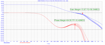
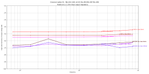
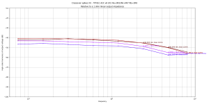
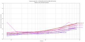
Inductive ceramic emitter resistors should be avoided in amplifiers. Here is their effect on open loop loop gain (resistor inductance from 0 to 200nH in 50nH steps):
As you can see, with an increase in inductance, the phase margin drops significantly.
As you can see, with an increase in inductance, the phase margin drops significantly.
Attachments
Last edited:
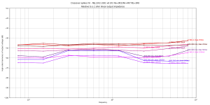
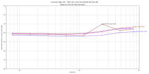
Inductive ceramic emitter resistors should be avoided in amplifiers. Here is their effect on open loop loop gain (resistor inductance from 0 to 200nH in 50nH steps):
As you can see, with an increase in inductance, the phase margin drops significantly.
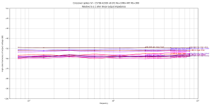
Yes, I will keep my 1nH SMD resistors, and they make the crossover much cleaner too.
What amp is this? 10MHz ULGF is pretty good!
Very interesting stuff! Even if I have not the knowledge to fully understand all of it.
All at all, I'm happy with what I'm reading compared to the amp I finished last year.
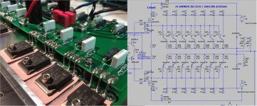
==> Fet Drivers + BJT output stage: positive premature results measured by you. Drivers running at about 130mA.
==> 7pairs of output devices : more devices were prefered over one. This combo gives about 12Wrms, which is more than sufficiënt for normal listening = no cross-over issues.
==> 0R22 Emitter resistors: could not reduce them further, heatsinks couldn't handle it. The lower Re, the better.
==> low inductance emitter resistors: well no info about this. I have installed vishay RS-2B 0R22 0.5% 3W. If anybody has an idea about the inductance of these... resistors.https://www.vishay.com/docs/30204/rsns.pdf
Looking forward to further investigations and conclusions.
All at all, I'm happy with what I'm reading compared to the amp I finished last year.
==> Fet Drivers + BJT output stage: positive premature results measured by you. Drivers running at about 130mA.
==> 7pairs of output devices : more devices were prefered over one. This combo gives about 12Wrms, which is more than sufficiënt for normal listening = no cross-over issues.
==> 0R22 Emitter resistors: could not reduce them further, heatsinks couldn't handle it. The lower Re, the better.
==> low inductance emitter resistors: well no info about this. I have installed vishay RS-2B 0R22 0.5% 3W. If anybody has an idea about the inductance of these... resistors.https://www.vishay.com/docs/30204/rsns.pdf
Looking forward to further investigations and conclusions.
Attachments
Last edited:
Next episode.
With the real low inductance resistors, results look much better.
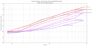
But I did not want to spend too much time comparing plots, so I came up with a metric. I noticed a strong correlation between the ugliness of the crossover spikes and the amplitude of the high harmonics (10th-50th). Below the 10th, it's more about static distortion, gm, hFe and all that. Above that order, the spikes dominate. So I just plotted the RMS sum of harmonics 10-50. This makes a synthetic plot from the measurements at various bias currents, frequencies, and output current.
For example, the difference between 0R33 and 0R15 emitter resistors is not clear from the first two scope style plots below:
With the real low inductance resistors, results look much better.
But I did not want to spend too much time comparing plots, so I came up with a metric. I noticed a strong correlation between the ugliness of the crossover spikes and the amplitude of the high harmonics (10th-50th). Below the 10th, it's more about static distortion, gm, hFe and all that. Above that order, the spikes dominate. So I just plotted the RMS sum of harmonics 10-50. This makes a synthetic plot from the measurements at various bias currents, frequencies, and output current.
For example, the difference between 0R33 and 0R15 emitter resistors is not clear from the first two scope style plots below:
Attachments
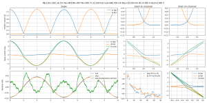
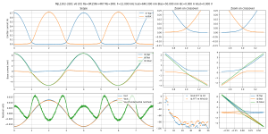
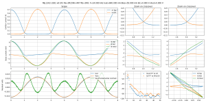
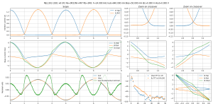
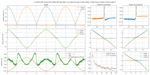
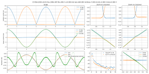
Basically the crossover zone where both transistors are ON has a certain "width", expressed in output current. It depends on bias current, but also on emitter resistor value. With high emitter resistors, the crossover is narrow, it is limited to the gm-doubling zone in the middle. With lower resistors, the exponential characteristic of BJTs comes into play and the crossover widens. This means the output current range where both transistors are ON widens with lower resistor values. In other words, you get more class A in your class AB for the same bias and idle power loss.
The important parameter for crossover spikes (and also other distortions) is that they worsen with high di/dt, and on a sinewave di/dt is highest at zero current. As the amplitude increases, the slope decreases, until the slope becomes zero at the top, before it goes the other way.
Thus widening the crossover means transistor turn-off will occur at a higher output current, thus at a lower slope point on the current waveform, a lower di/dt, which results in a smaller spike or no spike at all.
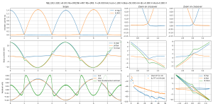
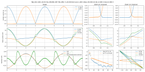
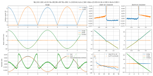
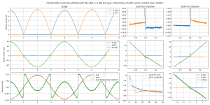
Here's an example: one plot for 0R15, one for 0R33.
In the 0R15 plot the crossover is wider, the transistors turn off at a higher total output current. The crossover spike is beginning to appear at this frequency, it manifests as a "bump" on the green curve (base current) on the left middle graph. As frequency or current increase this bump grows into a spike. With 0R15 ts just begins to appear, with 0R33 it is already beginning to sharpen a bit. The harmonics in the FFT plot reflect this.
The important parameter for crossover spikes (and also other distortions) is that they worsen with high di/dt, and on a sinewave di/dt is highest at zero current. As the amplitude increases, the slope decreases, until the slope becomes zero at the top, before it goes the other way.
Thus widening the crossover means transistor turn-off will occur at a higher output current, thus at a lower slope point on the current waveform, a lower di/dt, which results in a smaller spike or no spike at all.
Here's an example: one plot for 0R15, one for 0R33.
In the 0R15 plot the crossover is wider, the transistors turn off at a higher total output current. The crossover spike is beginning to appear at this frequency, it manifests as a "bump" on the green curve (base current) on the left middle graph. As frequency or current increase this bump grows into a spike. With 0R15 ts just begins to appear, with 0R33 it is already beginning to sharpen a bit. The harmonics in the FFT plot reflect this.
Attachments
-
 scope-Bias=50.000 mA Iout=640.000 mA F=12.000 kHz MJL1302-3281 v6 EF2 Re=0R33NI+4R7 Rb=3R8--MJL1.png275.5 KB · Views: 136
 -
 scope-Bias=50.000 mA Iout=640.000 mA F=12.000 kHz MJL1302-3281 v6 EF2 Re=0R15NI+4R7 Rb=3R8--MJL1.png272.9 KB · Views: 276
 -
 scope-Bias=50.000 mA Iout=640.000 mA F=24.000 kHz MJL1302-3281 v6 EF2 Re=0R15NI+4R7 Rb=3R8--MJL1.png285.7 KB · Views: 129
 -
 scope-Bias=50.000 mA Iout=640.000 mA F=24.000 kHz MJL1302-3281 v6 EF2 Re=0R33NI+4R7 Rb=3R8--MJL1.png284 KB · Views: 116
So, I said enough scope traces.
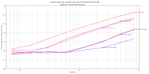
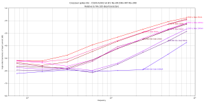
This is MJL1302/3281 biased at 50mA ; first two plots are with 0R33, they show the RMS sum of the high harmonics of output voltage, then the same calculation applied to input current on next plot.
Next two plots are with 0R15 emitter resistors. Unfortunately the test for 25mA bias didn't save the data so it is missing.
Text on the curves is bias and output current. X axis is frequency, Y is harmonics amplitude.
Red colors mean low bias, blue colors mean low output current.
At an output current of 2.56A, there is less difference between both values of resistors because the output current range is much larger than the crossover region. But at a lower peak current of 640mA, the wider crossover due to lower emitter resistors covers a much larger part of the actual output current, which means transistors turn off at a lower di/dt point, and the harmonics drop quite a lot.
Thermal stability is necessary of course, but there is probably a balance to find between the emitter resistor values that yield the flatter gm curve, and the lowest possible value for crossover spikes.
MOSFETs don't have this issue.
Attachments
-
 high-order-i--MJL1302-3281 v6 EF2 Re=0R33NI+4R7 Rb=3R8B=50.0m,F=12000,A=640.0m,V+=25.0,V-=25.0,V.png165.5 KB · Views: 350
 -
 high-order-i--MJL1302-3281 v6 EF2 Re=0R15NI+4R7 Rb=3R8B=100.0m,F=1500,A=2560.0m,V+=10.0,V-=10.0,.png120.2 KB · Views: 348
 -
 high-order-v--MJL1302-3281 v6 EF2 Re=0R15NI+4R7 Rb=3R8B=100.0m,F=1500,A=2560.0m,V+=10.0,V-=10.0,.png96.9 KB · Views: 343
 -
 high-order-v--MJL1302-3281 v6 EF2 Re=0R33NI+4R7 Rb=3R8B=50.0m,F=12000,A=640.0m,V+=25.0,V-=25.0,V.png130.5 KB · Views: 341
Last edited:
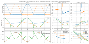
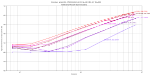
MJLs win against 2SC5200/A1943 in this test: high order harmonics are lower overall. Low orders are better too, because MJLs have better hFe linearity.
So I guess the MJLs keep the bipolar crown for now.
Using several MJL3281 in parallel is a bit overkill, so I wonder if the lower power versions (NJW0281 or something) would have better turn-off, or just the same if they're simply a lower area version of the same chip.
So I guess the MJLs keep the bipolar crown for now.
Using several MJL3281 in parallel is a bit overkill, so I wonder if the lower power versions (NJW0281 or something) would have better turn-off, or just the same if they're simply a lower area version of the same chip.
Attachments
-
 scope-Bias=25.000 mA Iout=2.560 A F=3.000 kHz MJL1302-3281 v6 EF2 Re=0R33NI+4R7 Rb=3R8--MJL1302-.png239.8 KB · Views: 112
 -
 scope-Bias=25.000 mA Iout=2.560 A F=3.000 kHz C5200-A1943 v6 EF2 Re=0R33NI+4R7 Rb=3R8--C5200-A19.png242.4 KB · Views: 115
 -
 scope-Bias=25.000 mA Iout=2.560 A F=48.000 kHz MJL1302-3281 v6 EF2 Re=0R33NI+4R7 Rb=3R8--MJL1302.png290.5 KB · Views: 117
 -
 scope-Bias=25.000 mA Iout=2.560 A F=48.000 kHz C5200-A1943 v6 EF2 Re=0R33NI+4R7 Rb=3R8--C5200-A1.png285 KB · Views: 335
 -
 high-order-i--C5200-A1943 v6 EF2 Re=0R15NI+4R7 Rb=3R8B=25.0m,F=6000,A=640.0m,V+=10.0,V-=10.0,Vo=.png167.7 KB · Views: 113
 -
 high-order-i--C5200-A1943 v6 EF2 Re=0R33NI+4R7 Rb=3R8B=50.0m,F=3000,A=1280.0m,V+=10.0,V-=10.0,Vo.png166.6 KB · Views: 111
Last edited:
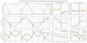
The TIPs were not as bad as I thought, unfortunately the high amount of distortion caused by the strong hFe droop on the PNP, and the bad matching between the two devices from different manufacturers... generated enough distortion to obscure the crossover spikes under study in the "sum of harmonics" plot.
Attachments
-
 scope-Bias=25.000 mA Iout=640.000 mA F=12.000 kHz TIP41C-42C v6 EF2 Re=0R33NI+4R7 Rb=3R8--TIP41C.png261.9 KB · Views: 117
 -
 scope-Bias=12.000 mA Iout=1.280 A F=12.000 kHz TIP41C-42C v6 EF2 Re=0R33NI+4R7 Rb=3R8--TIP41C-42.png250.1 KB · Views: 112
 -
 high-order-v--TIP41C-42C v6 EF2 Re=0R33NI+4R7 Rb=3R8B=25.0m,F=3000,A=640.0m,V+=10.0,V-=10.0,Vo=0.png93 KB · Views: 122
 -
 high-order-i--TIP41C-42C v6 EF2 Re=0R33NI+4R7 Rb=3R8B=25.0m,F=3000,A=640.0m,V+=10.0,V-=10.0,Vo=0.png73.9 KB · Views: 123
Last edited:
==> Fet Drivers + BJT output stage: positive premature results measured by you. Drivers running at about 130mA.
Nice build!
I will do more investigations on FETs as drivers, I think it's interesting.
I'm interested in knowing where you got these Sankens?
Nice build!
I will do more investigations on FETs as drivers, I think it's interesting.
I'm interested in knowing where you got these Sankens?
Transistors (Buy Online) | Profusion
Hi peufeu,
Many Carver power amps used 0R05 as emitter resistance. It was stable for bias current, but he used a pair of bias control circuits, one right at the outputs. TFM 4.0 would be a good model.
-Chris
Many Carver power amps used 0R05 as emitter resistance. It was stable for bias current, but he used a pair of bias control circuits, one right at the outputs. TFM 4.0 would be a good model.
-Chris
Thanks Bensen! Damn, it's special order only.
Just had a look at the schematic: it's a cascode output stage, so the output devices should have pretty low Vce, just a few volts from the way it's biased by diodes, which means very low dissipation in the output devices, so that would work. Nice find! I'm gonna try some new bias circuits, so I'm looking for inspiration...
Speaking of cascodes...
2SA2039/2SC5706 are tiny power transistors with a maximum power of 15W @ 25°C Tc, so they would need a cascode, the simplest would be a big bootstrapped MOSFET for example. But they do have some strong points...
- FBET/MBIT
- 5 amps max, high hFe (500) flat to 2 amps with good match between PNP and NPN
- 100MHz fT at 10mA, 300-400MHz up to 2A
- Adequate SOA for a cascoded transistor (3A at 5V Vce)
About 4 in parallel would make a pretty nice output stage already.
So how do they fare in the crossover spike test?...
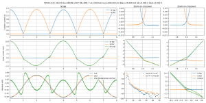
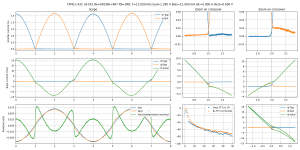
Test conditions:
One PNP, one NPN, at 5V Vce.
1R emitter resistors to keep the bias stable for the test, which makes crossover spikes much worse... in a real circuit lower resistors could be used.
Bias current set to 7mA, but it self heated to about 15mA to 20mA during the test.
Results are spectacular. At audio frequencies, crossover spikes completely disappear. I have to go to 24kHz at 2.56 amps to make them just begin to show up. And at 24kHz 640mA there are none. This is one pair of transistors, with a tiny bias. Four pairs in parallel to get the same current capability as MJL3281 would of course fare much better on this test, with higher flatter hFe and much higher bandwidth...
Hi peufeu,
Many Carver power amps used 0R05 as emitter resistance. It was stable for bias current, but he used a pair of bias control circuits, one right at the outputs. TFM 4.0 would be a good model.
-Chris
Just had a look at the schematic: it's a cascode output stage, so the output devices should have pretty low Vce, just a few volts from the way it's biased by diodes, which means very low dissipation in the output devices, so that would work. Nice find! I'm gonna try some new bias circuits, so I'm looking for inspiration...
Speaking of cascodes...
2SA2039/2SC5706 are tiny power transistors with a maximum power of 15W @ 25°C Tc, so they would need a cascode, the simplest would be a big bootstrapped MOSFET for example. But they do have some strong points...
- FBET/MBIT
- 5 amps max, high hFe (500) flat to 2 amps with good match between PNP and NPN
- 100MHz fT at 10mA, 300-400MHz up to 2A
- Adequate SOA for a cascoded transistor (3A at 5V Vce)
About 4 in parallel would make a pretty nice output stage already.
So how do they fare in the crossover spike test?...
Test conditions:
One PNP, one NPN, at 5V Vce.
1R emitter resistors to keep the bias stable for the test, which makes crossover spikes much worse... in a real circuit lower resistors could be used.
Bias current set to 7mA, but it self heated to about 15mA to 20mA during the test.
Results are spectacular. At audio frequencies, crossover spikes completely disappear. I have to go to 24kHz at 2.56 amps to make them just begin to show up. And at 24kHz 640mA there are none. This is one pair of transistors, with a tiny bias. Four pairs in parallel to get the same current capability as MJL3281 would of course fare much better on this test, with higher flatter hFe and much higher bandwidth...
Attachments
-
 scope-Bias=7.000 mA Iout=2.560 A F=24.000 kHz C5706-A2039 v6 EF2 Re=1RNI+4R7 Rb=3R8--C5706-A2039.png235.7 KB · Views: 162
 -
 scope-Bias=7.000 mA Iout=640.000 mA F=24.000 kHz C5706-A2039 v6 EF2 Re=1RNI+4R7 Rb=3R8--C5706-A2.png254.6 KB · Views: 151
 -
 high-order-i--C5706-A2039 v6 EF2 Re=1RNI+4R7 Rb=3R8B=25.0m,F=80000,A=2560.0m,V+=5.0,V-=5.0,Vo=0..png150.8 KB · Views: 152
 -
 high-order-v--C5706-A2039 v6 EF2 Re=1RNI+4R7 Rb=3R8B=25.0m,F=80000,A=2560.0m,V+=5.0,V-=5.0,Vo=0..png131.3 KB · Views: 142

Hi peufeu,
Well, they have more than that across them. But you're right in that the supply next up tracks the audio signal, keeping the supply constant up to the final commutator, which is way up at 118 ~ 125 VDC (bipolar supplies!).
I think there might be 40 VDC normally. I can't remember 'cause it isn't that important. If I need to know I look at the schematic. I have worked on these for decades - since they were new.
Another you would like would be the original Lightstar. The quiescent supply is 12.5 VDC approximately (bipolar) and it tracks the audio up to about 125 VDC bipolar. They use switching Mosfets at very high frequencies and call that a "down converter" using pulse width modulation. That drives a bunch of 2SA1302A and compliment output transistors. One of the very few parallel output type Carver designs. Sounded reasonably good. I had one for a while. I still have an output board burned out where the feedback resistor was because the reviewer did something really stupid that had nothing to do with listening to music. Canadian idiot who just simply tried to destroy the amplifier, and did one channel. They modified it soon after to make even stupidity less likely to hurt the amplifier.
A mark of all Carver amplifiers is to run efficiently, and to run cool. Some people don't like Bob Carver, but he is a very smart guy and accomplished quite a lot. I hate his terminology and advertising, but have a deep respect for his design abilities.
-Chris
Hi peufeu.... I'm gonna try some new bias circuits, so I'm looking for inspiration...
There was this idea Non-switching complimentary output stage
maybe you can get it working. Maybe two 9V batteries for the bootstrap supplies?
Nice work.
- Home
- Amplifiers
- Solid State
- Power amp OUTPUT STAGE measurements shootout