Thanks for the resistor idea. In my amplifier, the output transistors MJL3281 & MJL1302 were with a spread of about 30% in hFe. I selected this resistor with a nominal value of 4k7 and thereby equalized the collector currents in each arm with an accuracy of tens of microamperes.
Should you short/connect the emitters like that? Would it not be better to use separate resistors going to each emitter of the outputs?
Originally Posted by peufeu
I wonder if a lower impedance between the driver emitters would help both drivers control each transistor better.
What a lovely idea! Bravo, congratulations.
After playing with it a bit, it looks... complicated, because the famous spikes that occur at high di/dt do not come from lack of driving strength, they come from the power transistors having base base current inrush during turn-on and turn-off. This looks specific to BJT, the FETs don't do it, so it's probably related to BJT-specific stuff like charge storage.
This looks specific to BJT, the FETs don't do it.
Thank you for all the effort.
I am in the verge of ditching BJT output design, and using FETs instead.
BJT design just looks complicated even with 2EF. Too complicated to do it right.
Don't kid yourself. Designing a good output stage with FETs isn't easy either. The classic design using a pair of TO-92 driver transistors is just plain wrong. You have to address the characteristics of whatever output device you are using.
Then there is the rest of the amplifier ...
Then there is the rest of the amplifier ...
Switching distortion like this is due to turn-off, where the stored charge has to clear the device - with the EF output topology a speed-up cap is usually enough to tame this.Thank you for all the effort.
I am in the verge of ditching BJT output design, and using FETs instead.
BJT design just looks complicated even with 2EF. Too complicated to do it right.
With CFP topology there's no realistic way to speed-up switch-off and OS distortion tends to rise at HF from 5kHz or 10kHz or so - this means paying more attention to global feedback at higher frequencies to get good performance (ie advanced compensation schemes).
But the main thing to avoid is using slow transistors in the OS in the first place - 30MHz devices are often selected specifically because they have faster switch-off, not because that bandwidth is actually needed.
In the old days when 2N3055 and 2N2955's were the bees' knees CFP (or quasi-complementary) was a poor choice due to sluggish switch-off of these slow devices.
Having said all that its perfectly possible to get decent performance from CFP topology and it has the great advantage of running cool (low bias current) which extends equipment life and reliability.
My bias to FETs is solely to laterals which make thermal compensation unnecessary and greatly reduces the risk of secondary breakdown or thermal runaway due to bias drift over time.
Switching distortion like this is due to turn-off
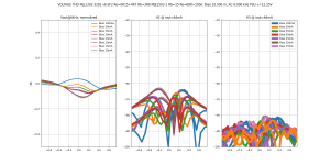
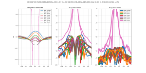
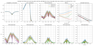
Look at the base current in the top right corner... There are 4 spikes per period: each turn-on and turn-off generates one. But these only appear on signals that are not realistic audio, like 1A at 48kHz, or several amps at 20kHz. At 12kHz, even with quite large current of 2.4A, no spikes. These come from di/dt, so to get rid of them, gotta parallel devices to reduce di/dt per device. These are strictly BJT and I think they're due to transit time.
These are different from the crossover spike you see in the THD residual of a complete amp that's operating properly (ie, not like in the previous case). These come from gm being different in the crossover zone, so there is only one per crossover instead of two here. And in fact, they don't really exist. Basically, at low current there is less gm, so the output signal is a bit "compressed", it has a bit less slope than it should... You can see it in the second graph, top row, middle plot, orange trace "Vout": near zero, it's like it's taking a break and lingering there. Or if it's gm-doubling, the slope increases and it looks like it accelerates through the crossover.
The THD residual removes the main sine wave, and the result shows a spike, but it isn't really one. It's just the way THD residual dusplays things.
CFP is different, it makes such a mess at turn-off that these appear tiny in comparison...
Attachments
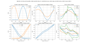
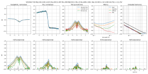
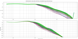
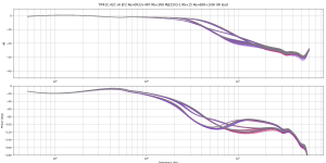
Now I'm going to compare MJL1302/3281 with several values of emitter resistors. They're all Ohmite TWW5.
Conditions:
The 4R7 SMD resistors that dampen the inductive wirewounds are still there.
Base resistors 3R8
Drivers MJE15030/15031 with 15R base resistors, 68R emitter resistor (~17mA idle)
100nF cap
Bias stability:
Values in the plot titles are what the bias was at the beginning of the test... With 0.15R emitter resistors, I noticed bias getting a bit wild. So, I halved the power supply voltage to sort of get the same amount of bias drift between 0R15 and 0R33. Anyway, accurate bias current to the mA is not that important, what matters is knowing whether it's optimally biased, underbiased, or overbiased/gm-doubling, and that's very visible in the measurements.
This stuff is well known, but let's recap:
Unlike MOSFETs, with BJT it does not pay to throw more bias current at it over the optimum level. Distortion at low current levels will change if the measurement is centered on zero, but my setup shows the distortion bumps just move around to a different value of output current, it's like playing whackamole. If you optimize THD on a low level signal, that will change the depth of the valley between the two peaks, but THD will not tell about the size of the peaks because it isn't going there...
In real music, low level signals very often ride on top of a higher amplitude signal like bass or another instrument playing, and that will sweep through the crossover so the low level signal of interest will be affected by the increase in distortion on either side. I believe this could be a source of "graininess" or that kind of stuff.
Anyway, emitter resistors.
Just open the pictures in tabs and flip through them : on the left is "basically gm", and the size of the mess is proportional to the emitter resistor.
X axis is "DC" output current.
The two other plots are harmonic H2 and H3. I left the others out because all the evens and all the odds look the same, only lower. I left the THD out because H3 hides H2 in the total, and their shape is different, so it's interesting to see both.
I've put all the bias values on the same picture, because otherwise that made too many plots to upload. It's a bit of a mess, so try squinting a bit.
Result: Emitter resistors are evil. They increase distortion dramatically.
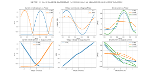
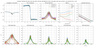
However, they are also necessary for stability: if you look at the gm plots with 0R15 resistors, 10-15-20mA are identical. That's because no matter what the setting was, it didn't care, and it self-heated to 20mA. That's with 12.5V Vce. Maybe my Vbe multiplier is at fault, but well.
So, basically, what this says is: use the lowest emitter resistor that gives a stable bias. This is true no matter what the bias is. "A higher emitter resistor is better for a lower bias setting" turns out to be a urban legend.
The point of a cascode output stage is to use lower emitter resistors by lowering Vce so it doesn't go into thermal runaway.
A cascode output stage therefore becomes an interesting option...
There's probably a FOM (figure of merit) for output stage power BJTs which would be something like fT divided by RthJH thermal resistance junction to heat sink. The former is about speed, RthJH is about lowering emitter resistor value without thermal runaway.
With 0R47 all biases have about equal peaks, but with 0R15 there is an optimum value, between the red and green curves, or 30-50 mA. That gives minimum distortion. Above that, gm-doubling occurs and it rises again, at different output currents.
Conditions:
The 4R7 SMD resistors that dampen the inductive wirewounds are still there.
Base resistors 3R8
Drivers MJE15030/15031 with 15R base resistors, 68R emitter resistor (~17mA idle)
100nF cap
Bias stability:
Values in the plot titles are what the bias was at the beginning of the test... With 0.15R emitter resistors, I noticed bias getting a bit wild. So, I halved the power supply voltage to sort of get the same amount of bias drift between 0R15 and 0R33. Anyway, accurate bias current to the mA is not that important, what matters is knowing whether it's optimally biased, underbiased, or overbiased/gm-doubling, and that's very visible in the measurements.
This stuff is well known, but let's recap:
Unlike MOSFETs, with BJT it does not pay to throw more bias current at it over the optimum level. Distortion at low current levels will change if the measurement is centered on zero, but my setup shows the distortion bumps just move around to a different value of output current, it's like playing whackamole. If you optimize THD on a low level signal, that will change the depth of the valley between the two peaks, but THD will not tell about the size of the peaks because it isn't going there...
In real music, low level signals very often ride on top of a higher amplitude signal like bass or another instrument playing, and that will sweep through the crossover so the low level signal of interest will be affected by the increase in distortion on either side. I believe this could be a source of "graininess" or that kind of stuff.
Anyway, emitter resistors.
Just open the pictures in tabs and flip through them : on the left is "basically gm", and the size of the mess is proportional to the emitter resistor.
X axis is "DC" output current.
The two other plots are harmonic H2 and H3. I left the others out because all the evens and all the odds look the same, only lower. I left the THD out because H3 hides H2 in the total, and their shape is different, so it's interesting to see both.
I've put all the bias values on the same picture, because otherwise that made too many plots to upload. It's a bit of a mess, so try squinting a bit.
Result: Emitter resistors are evil. They increase distortion dramatically.
However, they are also necessary for stability: if you look at the gm plots with 0R15 resistors, 10-15-20mA are identical. That's because no matter what the setting was, it didn't care, and it self-heated to 20mA. That's with 12.5V Vce. Maybe my Vbe multiplier is at fault, but well.
So, basically, what this says is: use the lowest emitter resistor that gives a stable bias. This is true no matter what the bias is. "A higher emitter resistor is better for a lower bias setting" turns out to be a urban legend.
The point of a cascode output stage is to use lower emitter resistors by lowering Vce so it doesn't go into thermal runaway.
A cascode output stage therefore becomes an interesting option...
There's probably a FOM (figure of merit) for output stage power BJTs which would be something like fT divided by RthJH thermal resistance junction to heat sink. The former is about speed, RthJH is about lowering emitter resistor value without thermal runaway.
With 0R47 all biases have about equal peaks, but with 0R15 there is an optimum value, between the red and green curves, or 30-50 mA. That gives minimum distortion. Above that, gm-doubling occurs and it rises again, at different output currents.
Attachments
-
 gthd-6k--MJL1302-3281 v6 EF2 Re=0R47+4R7 Rb=3R8 MJE1503-1 Rb=15 Re=68R+100nB=10.0m,HA=4.0m,LA=25.png230.9 KB · Views: 291
 -
 gthd-6k--MJL1302-3281 v6 EF2 Re=0R33+4R7 Rb=3R8 MJE1503-1 Rb=15 Re=68R+100nB=10.0m,HA=4.0m,LA=25.png218.5 KB · Views: 292
 -
 gthd-6k--MJL1302-3281 v6 EF2 Re=0R15+4R7 Rb=3R8 MJE1503-1 Rb=15 Re=68R+100nB=10.0m,HA=4.0m,LA=25.png210 KB · Views: 285
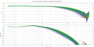
Full plots of the best (0R15,30mA) and worst (0R47,20mA) case:
High order harmonics fall off much quicker with the lower emitter resistor value. I'm not posting all the other plots, but the same happens at all bias values. Lower emitter resistors gives lower THD, faster high order harmonics fall off, at all biases.
High order harmonics fall off much quicker with the lower emitter resistor value. I'm not posting all the other plots, but the same happens at all bias values. Lower emitter resistors gives lower THD, faster high order harmonics fall off, at all biases.
Attachments
Last edited:
Hi peufeu,
Yes, that is what I have found wrt emitter resistors. Multiple output pairs tend to reduce individual current variations with signal (obvious) and may be one reason why some higher powered amplifiers perform better than low power ones.
Notice I did not say "sounds better", because once you open that can of worms, all kinds of junk would be trotted out as "sounding better". There is no accounting for taste in some folks. I am specifically thinking about things like the NAD 3020. The Naim Nate is also a horrible creation the some people love. These clearly have compromised performance.
-Chris
Now, suppose we have two pairs of devices, then we have two ways of using them:
- Put one on top of the other for a cascode and use 0R15 resistors...
- Or put them in parallel with 0R33 resistors each.
We will never know because I ran the parallel test with 0R47 resistors 😀
So... compare below plot with first one in this post.
For the parallel test, since I have only one pair of devices on the setup, I simply double the load resistor (8R to 16R). This does not model the doubling in input capacitance, but that doesn't matter for this test. So each device has half the current.
The left plot is not actually gm, it is the variations in amplitude of output voltage due to variations in gm. With the halving of current, these variations are also halved, and the graph shows that.
The result is about 10dB lower distortion, so could be a good investment... but it is not better than just lowering the emitter resistors.
I will do the parallel test with 0R15 resistors later, because there is a 2SC5200/2SA1943 on the setup now.
Attachments

Last edited:
Hi peufeu,
Yes, exactly.
Stacked outputs have many other advantages in reliability where SOA is concerned, as well as some schemes where the Vce is held approximately constant (Carver). But for the purposes of output stage distortion, these designs are a distraction. I don`t think we should consider them from a distortion perspective.
-Chris
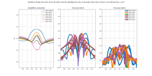
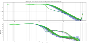
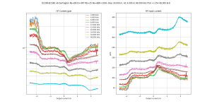
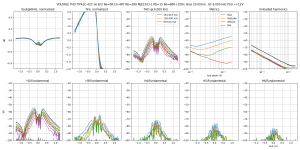
Input current, MJL versus C5200/A1943...
hfe mismatch is a bit worse for the Sankens, they most likely gave the PNP higher gain to compensate for beta droop at high current, which the MJLs do not exhibit.
I don't need huge power or SOA, so the reason I consider it is purely to get away with lower value emitter resistors. Another biasing scheme could also work, there is no shortage of those... Do they work, that's another question...
hfe mismatch is a bit worse for the Sankens, they most likely gave the PNP higher gain to compensate for beta droop at high current, which the MJLs do not exhibit.
Stacked outputs have many other advantages in reliability where SOA is concerned, as well as some schemes where the Vce is held approximately constant (Carver). But for the purposes of output stage distortion, these designs are a distraction. I don`t think we should consider them from a distortion perspective.
I don't need huge power or SOA, so the reason I consider it is purely to get away with lower value emitter resistors. Another biasing scheme could also work, there is no shortage of those... Do they work, that's another question...
Attachments
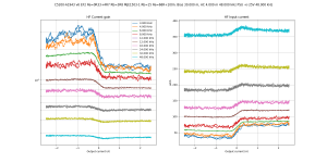

Distortion with 0R33 emitter resistors is exactly the same between MJLs and the Sankens.
Looks like there was a bug with the one bias value on the right plot, oh well.
Firing up the network analyzer...
Looks like there was a bug with the one bias value on the right plot, oh well.
Firing up the network analyzer...
Attachments

Last edited:
Cue the epic soundtrack 😀
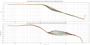
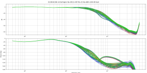
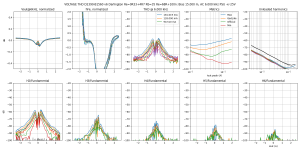
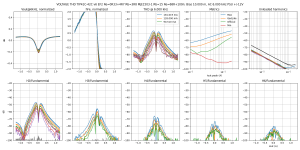
They don't like low base resistor values, 20R is the minimum, below that there is a bump at 1MHz. So some optimization is needed. For now, 15R base resistors for the drivers, 20R for A5200/C1943, plus a ferrite bead, which may be unnecessary.
I had to measure the MJLs again to make sure, but yeah, it's true:
A5200/C1943 are much faster... They are faster than both lateral and vertical MOSFETs too.
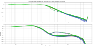
First graph shows Vce from 5V to 25V and various DC output current: remarkably consistent, which should make compensation easy, because there is no worst case.
Second graph shows a sweep of DC output current at 25V Vce, same thing.
Third graph shows several values of bias: same thing.
Lath three graphs are MJL, ALFET Laferal FETs, and IRFP240/9240.
The most amazing thing is the phase at 10MHz and above. Where is that second pole?
I need faster drivers.
They don't like low base resistor values, 20R is the minimum, below that there is a bump at 1MHz. So some optimization is needed. For now, 15R base resistors for the drivers, 20R for A5200/C1943, plus a ferrite bead, which may be unnecessary.
I had to measure the MJLs again to make sure, but yeah, it's true:
A5200/C1943 are much faster... They are faster than both lateral and vertical MOSFETs too.
First graph shows Vce from 5V to 25V and various DC output current: remarkably consistent, which should make compensation easy, because there is no worst case.
Second graph shows a sweep of DC output current at 25V Vce, same thing.
Third graph shows several values of bias: same thing.
Lath three graphs are MJL, ALFET Laferal FETs, and IRFP240/9240.
The most amazing thing is the phase at 10MHz and above. Where is that second pole?
I need faster drivers.
Attachments
-
 C5200-A1943 v6 EF2 Re=0R33+4R7 Rb=20 MJE1503-1 Rb=15 Re=68R+100n load.png223.7 KB · Views: 369
 -
 C5200-A1943 v6 EF2 Re=0R33+4R7 Rb=20 MJE1503-1 Rb=15 Re=68R+100n 25V load.png171.6 KB · Views: 134
 -
 C5200-A1943 v6 EF2 Re=0R33+4R7 Rb=20 MJE1503-1 Rb=15 Re=68R+100n 25V no_load.png122.9 KB · Views: 132
 -
 IRFP240-9240 v4 Re=0R15+4R7 Rb=130 2N3904-6 Rg=20R+FB load.png368.1 KB · Views: 126
 -
 ALFET v3 Re=0R Rb=20+FB Rdrive=4700 NoThiele No50R load.png354.4 KB · Views: 122
 -
 MJL1302-3281 v6 EF2 Re=0R33+4R7 Rb=6R8 MJE1503-1 Rb=15 Re=68R+100n load.png357.4 KB · Views: 124
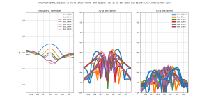
I will go through the backlog of devices I wanted to test...
2SD2390-2SB1560, darlingtons from Sanken.
Frequency response is nothing to write home about, and phase shift is quite large. This leads to the usual ULGF in the MHz range. Not for a high bandwidth amp.
Current gain and input current do weird things, the P and N are not well matched.
Distortion is pretty much the same as a DIY darlington with a pair of BJTs.
This is an industrial cost saving measure, to save the labor of affixing drivers to the heatsink. EF2 wins.
Attachments
-
 D2390-B1560 v6 Darlington Re=0R33+4R7 Rb=35 Re=68R+100n load.png301.7 KB · Views: 117
 -
 incurrent--D2390-B1560 v6 Darlington Re=0R33+4R7 Rb=35 Re=68R+100nB=30.0m,HA=4.0m,LA=2500.0m,THD.png308.6 KB · Views: 112
 -
 thd-F=6k-D2390-B1560 v6 Darlington Re=0R33+4R7 Rb=35 Re=68R+100nB=15.0m,HA=4.0m,LA=2500.0m,THDF=.png275.1 KB · Views: 108
Last edited:
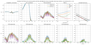
Another flavor: TIP41C from ST and TIP42C from OnSemi
These are cheap low-fT TO-220 transistors, specified for pretty high current for the size. I used the same setup, 20R base resistors, and MJE15030/1 as drivers with 15R base resistors.
Current gain is not well matched. Both PNP and NPN suffer from pretty strong beta droop at high current. The PNP has higher gain and higher droop.
They're TO-220s, which means low thermal mass. The Vbe multiplier had trouble keeping the bias in line, and all the tests ended up were overbiased. I guess this is because it was designed for TO-247 and the sensor is thermally coupled to the center leg of the transistor which is part of the leadframe and directly connected to the chip, but apparently that doesn't work well with TO-220s.
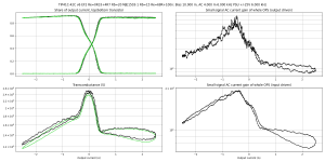
Self-heating is visible in the graphs: the gm plot has "loops" on both sides.
This test uses 40Hz to set the "DC" current, and measures "AC" parameters on each point along this wave. This means the entire graph is actually a loop. If the transistor has the same parameters while current goes up than when it goes down, the loop looks like a single curve because both directions measure the same and display on top of each other. However, on the high current portion of this waveform, the transistor has enough time (a few milliseconds) to heat up enough that it gives a completely different measurement on the way back, although the current is the same.
As it heats up, hFe and bias move all over the place ; this plus the hFe droop causes a rather spectacular rise in distortion on the harmonics plot:
I'm really glad profdc9 talked me into testing these transistors, because I've been quite interested in these kinds of distortions too.
To have mercy for these poor transistors, I'm running the test again at half the current and half the Vce, and since they did not oscillate, with much lower base resistors too.
These are cheap low-fT TO-220 transistors, specified for pretty high current for the size. I used the same setup, 20R base resistors, and MJE15030/1 as drivers with 15R base resistors.
Current gain is not well matched. Both PNP and NPN suffer from pretty strong beta droop at high current. The PNP has higher gain and higher droop.
They're TO-220s, which means low thermal mass. The Vbe multiplier had trouble keeping the bias in line, and all the tests ended up were overbiased. I guess this is because it was designed for TO-247 and the sensor is thermally coupled to the center leg of the transistor which is part of the leadframe and directly connected to the chip, but apparently that doesn't work well with TO-220s.
Self-heating is visible in the graphs: the gm plot has "loops" on both sides.
This test uses 40Hz to set the "DC" current, and measures "AC" parameters on each point along this wave. This means the entire graph is actually a loop. If the transistor has the same parameters while current goes up than when it goes down, the loop looks like a single curve because both directions measure the same and display on top of each other. However, on the high current portion of this waveform, the transistor has enough time (a few milliseconds) to heat up enough that it gives a completely different measurement on the way back, although the current is the same.
As it heats up, hFe and bias move all over the place ; this plus the hFe droop causes a rather spectacular rise in distortion on the harmonics plot:
I'm really glad profdc9 talked me into testing these transistors, because I've been quite interested in these kinds of distortions too.
To have mercy for these poor transistors, I'm running the test again at half the current and half the Vce, and since they did not oscillate, with much lower base resistors too.
Attachments
-
 incurrent--TIP41C-42C v6 EF2 Re=0R33+4R7 Rb=20 MJE1503-1 Rb=15 Re=68R+100nB=20.0m,HA=4.0m,LA=250.png377.8 KB · Views: 109
 -
 thd-F=6k-TIP41C-42C v6 EF2 Re=0R33+4R7 Rb=20 MJE1503-1 Rb=15 Re=68R+100nB=10.0m,HA=4.0m,LA=2500..png356.1 KB · Views: 118
 -
 gm-F=6k-TIP41C-42C v6 EF2 Re=0R33+4R7 Rb=20 MJE1503-1 Rb=15 Re=68R+100nB=10.0m,HA=4.0m,LA=2500.0.png212.5 KB · Views: 105
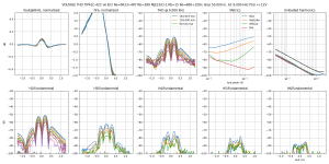
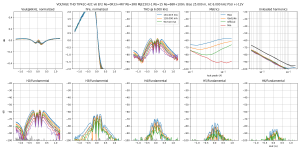
And here it is
Vce 12V
Rb 3.8R
Ipeak 1.25A
Peak thermal power is 4x less, so self heating is no longer visible, there is less distortion, and the bias is under control. But the PNP is still having trouble at high current, which causes a rise in H2 (bottom left corner of all the pics).
Here are the results at various biases.
Attachments
-
 thd-F=6k-TIP41C-42C v6 EF2 Re=0R33+4R7 Rb=3R8 MJE1503-1 Rb=15 Re=68R+100nB=50.0m,HA=4.0m,LA=1250.png299.1 KB · Views: 90
 -
 thd-F=6k-TIP41C-42C v6 EF2 Re=0R33+4R7 Rb=3R8 MJE1503-1 Rb=15 Re=68R+100nB=35.0m,HA=4.0m,LA=1250.png297.9 KB · Views: 91
 -
 thd-F=6k-TIP41C-42C v6 EF2 Re=0R33+4R7 Rb=3R8 MJE1503-1 Rb=15 Re=68R+100nB=30.0m,HA=4.0m,LA=1250.png293.1 KB · Views: 87
 -
 thd-F=6k-TIP41C-42C v6 EF2 Re=0R33+4R7 Rb=3R8 MJE1503-1 Rb=15 Re=68R+100nB=25.0m,HA=4.0m,LA=1250.png293.3 KB · Views: 96
 -
 thd-F=6k-TIP41C-42C v6 EF2 Re=0R33+4R7 Rb=3R8 MJE1503-1 Rb=15 Re=68R+100nB=20.0m,HA=4.0m,LA=1250.png296.1 KB · Views: 97
 -
 thd-F=6k-TIP41C-42C v6 EF2 Re=0R33+4R7 Rb=3R8 MJE1503-1 Rb=15 Re=68R+100nB=10.0m,HA=4.0m,LA=1250.png308.2 KB · Views: 93
 -
 thd-F=6k-TIP41C-42C v6 EF2 Re=0R33+4R7 Rb=3R8 MJE1503-1 Rb=15 Re=68R+100nB=15.0m,HA=4.0m,LA=1250.png303.5 KB · Views: 86
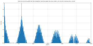
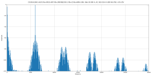
Of course it is also possible to look at it using FFT.
This contains exactly the same information as the graphs posted above, in a much less human-readable form 😀
I remember someone saying "but but but if there was self heating distortion in the output stage, then there would be intermodulation between a low frequency tone and a high frequency tone!"
Well, the input signal consists of only 40Hz, 80Hz, and 6kHz. All the rest is distortion...
Attachments
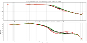
I forgot the current gain.
With the MJL's the output driven current gain is 15000 (NPN)-40000(PNP) ; knowing the power transistors have hFe of 100 and 125 this gives 150 and 320 for the drivers.
The TIPs post a total current gain of flat 10000 for the NPN, so dividing by the driver gain gives hFe of 66 for the TIP which agrees with the datasheet. The PNP has hFe 180 at low current and 62 at 1A.
I noticed that I got the NPN from ST and the PNP from OnSemi... And the ST datasheet says:
So it could be possible that the TIP42C from ST would have the same good hFe linearity as their TIP41C. I would avoid the ones from ON, hFe droop is terrible.
And now the moneyshot 😀
WTF, TIP41C/TIP42C with a ridiculous fT of 3MHz, post a better frequency response than MJL3281?
I think there is an explanation: the cost for MJL3281/MJL1302 huge SOA is a correspondingly huge collector to base capacitance of 600pF, whereas the much smaller TIPs have 10x less.
2SC5200 and 2SA1943 also have only 200pF which is very good considering they're almost as beefy as the MJLs.
Also the high fT of MJLs is only enabled at several amps.
So as frequency rises, with the MJLs, the high capacitance sucks all the base current to the collector, whereas with the other lower capacitance transistors, enough current goes through the base-emitter capacitance and into the output to pretend it's still working, while it is not actually providing any gain, it's just sitting there acting as a capacitor... through which the drivers (MJE15030/31) drive the output via the very low base resistor. To test this I increased the base resistor from 6.8 ohms to 20 ohms, and the frequency response dropped. So this will only work with fast drivers, and if the output is isolated from a capacitive load.
Therefore, for my high-bandwidth amplifier project, with a correspondingly ridiculous unity gain crossover frequency, I must take care to select outputs with low collector capacitance...
Time for shopping! Are there any BJTs like 2SC5200 but with lower capacitance?
With the MJL's the output driven current gain is 15000 (NPN)-40000(PNP) ; knowing the power transistors have hFe of 100 and 125 this gives 150 and 320 for the drivers.
The TIPs post a total current gain of flat 10000 for the NPN, so dividing by the driver gain gives hFe of 66 for the TIP which agrees with the datasheet. The PNP has hFe 180 at low current and 62 at 1A.
I noticed that I got the NPN from ST and the PNP from OnSemi... And the ST datasheet says:
New enhanced series
■ High switching speed
■ hFE improved linearity
Applications
■ Audio amplifier
The TIP41C is a base island technology NPN power transistor in TO-220 plastic package that make this device suitable for audio, power linear
and switching applications.
So it could be possible that the TIP42C from ST would have the same good hFe linearity as their TIP41C. I would avoid the ones from ON, hFe droop is terrible.
And now the moneyshot 😀
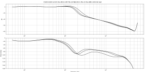
WTF, TIP41C/TIP42C with a ridiculous fT of 3MHz, post a better frequency response than MJL3281?
I think there is an explanation: the cost for MJL3281/MJL1302 huge SOA is a correspondingly huge collector to base capacitance of 600pF, whereas the much smaller TIPs have 10x less.
2SC5200 and 2SA1943 also have only 200pF which is very good considering they're almost as beefy as the MJLs.
Also the high fT of MJLs is only enabled at several amps.
So as frequency rises, with the MJLs, the high capacitance sucks all the base current to the collector, whereas with the other lower capacitance transistors, enough current goes through the base-emitter capacitance and into the output to pretend it's still working, while it is not actually providing any gain, it's just sitting there acting as a capacitor... through which the drivers (MJE15030/31) drive the output via the very low base resistor. To test this I increased the base resistor from 6.8 ohms to 20 ohms, and the frequency response dropped. So this will only work with fast drivers, and if the output is isolated from a capacitive load.
Therefore, for my high-bandwidth amplifier project, with a correspondingly ridiculous unity gain crossover frequency, I must take care to select outputs with low collector capacitance...
Time for shopping! Are there any BJTs like 2SC5200 but with lower capacitance?
Attachments
Last edited:
Check out post #8 of this thread. Winfield Hill (co-author of "The Art Of Electronics") gives his own Figure Of Merit for ranking power transistors when building fast amplifiers.
Winfield's 100W DC-10MHz 1000V/us amplifier
Winfield's 100W DC-10MHz 1000V/us amplifier
- Home
- Amplifiers
- Solid State
- Power amp OUTPUT STAGE measurements shootout