Pd/Cob is a good FOM. If I use a big MOSFET as a cascode, it could also be (max Ie for flat hFe)/Cob.
MT88
Can you tell us about this, we may need to put it in its own thread. (I have temporarily deleted your post , you may PM if necessary.)
Can you tell us about this, we may need to put it in its own thread. (I have temporarily deleted your post
, you may PM if necessary.)Whether his FOM was wise or stupid, the final amplifier which resulted, was excellent.
It's absolutely wise.
While the TIPs are on the test fixture I am going to run the transient test to see if the lower fT implies worse switching spikes. These spikes should be related to transit time and not fT, though.
I will then do the same with the C5200/A1943 to compare with MJL's.
It's running. I will also include some pretty fast BJTs for comparison: a "thermally enhanced" pair of A2039/C5706
Attachments
Last edited:
Just a stupid question that came to mind: As I understand it, you're seeing oscillations and use base resistors to tame them, but could the test setup be improved to avoid them? Do you for example have decoupling caps on the supplies close to the transistors?
On the one hand, this setup has low power supply inductance, because the decoupling caps are next to the devices, but that doesn't remove the inductance of the leads, which is significant on TO-247...
On the other hand, being a test setup adds a bit of inductance for convenience: the resistors are on headers to easily change them. Also on a real board the device leads would be shorter, but I can't do that because then there wouldn't be enough room to aim a soldering iron in there.
On the other hand, being a test setup adds a bit of inductance for convenience: the resistors are on headers to easily change them. Also on a real board the device leads would be shorter, but I can't do that because then there wouldn't be enough room to aim a soldering iron in there.
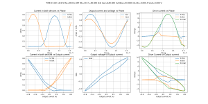
I simulated a simple open loop class AB current amplifier, and I found the same rough order-of-magnitude distortion that peufeu did. However, I don't think the simulation includes thermal variations. Another thing I found that might be interesting to check is that the distortion seems to be dominated by crossover distortion. I guess this is not surprising given that it is open loop. The DC quiescent point for zero voltage output with no signal is tricky to get because there is no feedback to set it.
.
.
Nice!
As for the DC operating point, I'd recommend to step it so you get a DC output current from -4x to 4x your bias current setting. You can do that with a DC current source at the output, or just step the DC input voltage. Then it will show at what DC output current you get maximum THD. The result should look like the THD vs output current plots I posted earlier.
As for the DC operating point, I'd recommend to step it so you get a DC output current from -4x to 4x your bias current setting. You can do that with a DC current source at the output, or just step the DC input voltage. Then it will show at what DC output current you get maximum THD. The result should look like the THD vs output current plots I posted earlier.
You could also insert a DC servo to keep the output DC stable and zero. This does not impact the AC measurements.
Jan
Jan
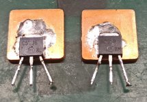
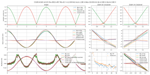
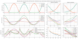
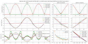
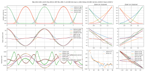
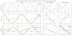
I've run the "crossover spike test" using the oscilloscope on the following devices:
TIP41C/TIP42C at lower Vce
MJL1302/3281
C5200/A1943
C5706/A2039 "ghetto thermally enhanced" at low Vce
I ran them without any drivers, so we can know that the spikes that will appear on the graphs don't come from the drivers.
Speaking about that, I think I was wrong earlier: all these graphs show only one spike per crossover and it is at turn-off. The previous plot (with drivers) that showed two spikes per crossover made me conclude there was one at turn-on and one at turn-off, but that may be an interaction with the drivers instead. TBD.
MJL1302/3281 are first in line, with 3R8 and 20R resistors... The base resistor doesn't seem to change the energy of the turn-off spike. With a higher value, it is lower and longer. With a lower value, it is shorter and spikier.
The annoying thing is it begins to show signs of turn-off problems at 6kHz, 2.5A which is not that high in frequency... One more reason to use several parallel devices to reduce di/dt per device.
Attachments
-
 scope-Bias=50.000 mA Iout=1.280 A F=12.000 kHz MJL1302-3281 v6 EF2 Re=0R33+4R7 Rb=3R8--MJL1302-3.png363.2 KB · Views: 358
 -
 scope-Bias=50.000 mA Iout=2.560 A F=6.000 kHz MJL1302-3281 v6 EF2 Re=0R33+4R7 Rb=3R8--MJL1302-32.png342.9 KB · Views: 353
 -
 scope-Bias=50.000 mA Iout=2.560 A F=3.000 kHz MJL1302-3281 v6 EF2 Re=0R33+4R7 Rb=3R8--MJL1302-32.png327.7 KB · Views: 354
 -
 scope-Bias=50.000 mA Iout=2.560 A F=48.000 kHz MJL1302-3281 v6 EF2 Re=0R33+4R7 Rb=3R8--MJL1302-3.png414 KB · Views: 362
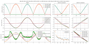
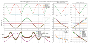
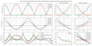
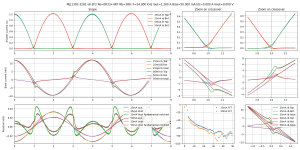
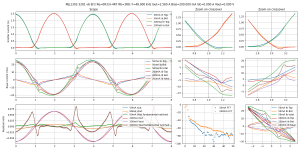
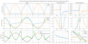
Now, MJLs versus C5200/A1943... both with 20R base resistors because I forgot to change them.
The difference begins to show up at 6kHz 1.2A. Below that the plots look the same.
While the C5200 appeared faster in the frequency response test, MJLs strike back with much lower crossover spikes... The tiny FFT plot shows quite a difference. Is there a point to look at harmonics 20-50 of a 12kHz tone, who knows, but the shapness of that spike certainly shows.
This plus the much better hFe linearity of the MJL's means they stay on top.
Attachments
-
 scope-Bias=50.000 mA Iout=1.280 A F=24.000 kHz C5200-A1943 v6 EF2 Re=0R33+4R7 Rb=20--C5200-A1943.png399.4 KB · Views: 128
 -
 scope-Bias=50.000 mA Iout=1.280 A F=12.000 kHz C5200-A1943 v6 EF2 Re=0R33+4R7 Rb=20--C5200-A1943.png351.4 KB · Views: 320
 -
 scope-Bias=50.000 mA Iout=1.280 A F=6.000 kHz C5200-A1943 v6 EF2 Re=0R33+4R7 Rb=20--C5200-A1943 .png314.3 KB · Views: 137
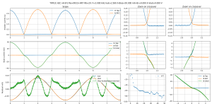
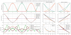
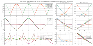
MJLs versus TIP41-42.
It would not be fair to compare them at the same current, because an amp using TIP41-42 would use many more devices. So I will compare 4 TIP pairs with one MJL pair, by running the TIPs at 1/4 the current.
And... lol, I forgot to set the bias to 1/4 for the TIPs, so since I ran all the tests at 50mA bias, we're comparing 4 TIPs at 50mA each with one MJL at 50mA, which is completely bogus. Bias influences this test a lot, because the transistor that is turning off will do so much slower when higher bias makes the class-A region wider.
I set it to run, meanwhile I will post the rest of the plots.
So here are just TIPs at a variety of frequencies and current. At 1.28A they begin to have turn off problems at 1.5kHz, and this is with a bias current that is way too high.
A2039/C5706 self-heated to 150mA bias too, so I won't post the results. Will run that one again.
Attachments
-
 scope-Bias=50.000 mA Iout=2.560 A F=1.500 kHz TIP41C-42C v6 EF2 Re=0R33+4R7 Rb=20--TIP41C-42C v6.png220.6 KB · Views: 129
 -
 scope-Bias=50.000 mA Iout=2.560 A F=3.000 kHz TIP41C-42C v6 EF2 Re=0R33+4R7 Rb=20--TIP41C-42C v6.png225.3 KB · Views: 123
 -
 scope-Bias=50.000 mA Iout=1.280 A F=12.000 kHz TIP41C-42C v6 EF2 Re=0R33+4R7 Rb=20--TIP41C-42C v.png243.4 KB · Views: 113
 -
 xy-Bias=50.000 mA Iout=640.000 mA F=12.000 kHz TIP41C-42C v6 EF2 Re=0R33+4R7 Rb=20--TIP41C-42C v.png189.4 KB · Views: 108
 -
 xy-Bias=50.000 mA Iout=640.000 mA F=48.000 kHz TIP41C-42C v6 EF2 Re=0R33+4R7 Rb=20--TIP41C-42C v.png205.6 KB · Views: 107
Last edited:
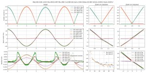
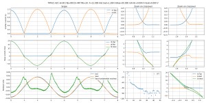
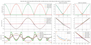
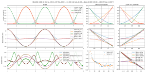
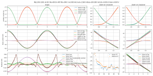
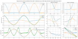
This is the TIPs versus the MJLs, at the same total simulated bias.
One TIPs at 50mA bias, with one quarter the current.
MJLs at 200mA bias.
Both have 0R33 emitter resistors.
An interesting thing happens: the TIPs, being much slower, produce a much longer crossover spike but it is soft. MJLs produce a sharper shorter spike.
This looks a lot like diode recovery (someone mentioned it there) with TIPs having slow soft recovery, and MJLs having fast hard recovery at turn-off.
While MJLs clearly beat C5200/A1943, It is not clear who wins this one...
Attachments
-
 scope-Bias=200.000 mA Iout=2.560 A F=48.000 kHz MJL1302-3281 v6 EF2 Re=0R33+4R7 Rb=3R8--MJL1302-.png430.8 KB · Views: 115
 -
 scope-Bias=200.000 mA Iout=2.560 A F=24.000 kHz MJL1302-3281 v6 EF2 Re=0R33+4R7 Rb=3R8--MJL1302-.png402 KB · Views: 122
 -
 scope-Bias=200.000 mA Iout=2.560 A F=12.000 kHz MJL1302-3281 v6 EF2 Re=0R33+4R7 Rb=3R8--MJL1302-.png377.7 KB · Views: 130
MJLs with 0R33 resistors, 25mA bias vs 50mA bias.
Lower bias value worsens crossover turn-off (and corresponding high harmonics).
Lower bias value worsens crossover turn-off (and corresponding high harmonics).
Attachments
-
 scope-Bias=50.000 mA Iout=1.280 A F=6.000 kHz MJL1302-3281 v6 EF2 Re=0R33+4R7 Rb=3R8--MJL1302-32.png326.2 KB · Views: 113
 -
 scope-Bias=50.000 mA Iout=1.280 A F=12.000 kHz MJL1302-3281 v6 EF2 Re=0R33+4R7 Rb=3R8--MJL1302-3.png342.2 KB · Views: 109
 -
 scope-Bias=50.000 mA Iout=1.280 A F=24.000 kHz MJL1302-3281 v6 EF2 Re=0R33+4R7 Rb=3R8--MJL1302-3.png370.6 KB · Views: 104
MJLs at 50 mA versus 200mA.
Increased bias does help, but only a little bit. So this is the same as with the distortion test: with BJTs it is not profitable to bias above the optimum current.
Increased bias does help, but only a little bit. So this is the same as with the distortion test: with BJTs it is not profitable to bias above the optimum current.
Attachments
-
 scope-Bias=50.000 mA Iout=1.280 A F=6.000 kHz MJL1302-3281 v6 EF2 Re=0R33+4R7 Rb=3R8--MJL1302-32.png366.2 KB · Views: 96
 -
 scope-Bias=50.000 mA Iout=1.280 A F=12.000 kHz MJL1302-3281 v6 EF2 Re=0R33+4R7 Rb=3R8--MJL1302-3.png391.4 KB · Views: 95
 -
 scope-Bias=50.000 mA Iout=1.280 A F=24.000 kHz MJL1302-3281 v6 EF2 Re=0R33+4R7 Rb=3R8--MJL1302-3.png406.8 KB · Views: 97
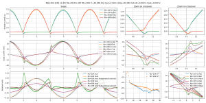
One MJL at 200mA bias
versus 4x MJL at 50mA bias (just one really, but the current is scaled).
All with 0R33 resistors.
Using parallel devices gives a spectacular improvement in crossover spikes by reducing per-device di/dt, even though the total bias current budget is the same.
(although four of these are going to be a bit expensive, but maybe two)
Attachments
-
 scope-Bias=200.000 mA Iout=2.560 A F=48.000 kHz MJL1302-3281 v6 EF2 Re=0R33+4R7 Rb=3R8--MJL1302-.png420.7 KB · Views: 110
 -
 scope-Bias=200.000 mA Iout=2.560 A F=24.000 kHz MJL1302-3281 v6 EF2 Re=0R33+4R7 Rb=3R8--MJL1302-.png392.6 KB · Views: 116
 -
 scope-Bias=200.000 mA Iout=2.560 A F=12.000 kHz MJL1302-3281 v6 EF2 Re=0R33+4R7 Rb=3R8--MJL1302-.png361.5 KB · Views: 121
 -
 scope-Bias=200.000 mA Iout=2.560 A F=6.000 kHz MJL1302-3281 v6 EF2 Re=0R33+4R7 Rb=3R8--MJL1302-3.png340.3 KB · Views: 119
Last edited:
I switched emitter resistors to 0R15 and had a WTF moment 😀
This is 0R15 with 100mA bias versus 0R33 with 25mA bias. The difference is huge, and 100mA bias is much worse, whereas it should not!...
Since emitter resistors are evil, I suspected them and measured the inductance of both 0R15 resistors and found them to be what I expected, about 200nH...
I started another test with non-inductive DIY emitter resistors.
Attachments
It looks very much better with the non-inductive resistors (compare with previous post).
Conclusion #1: the previous measurements are actually suspicious, damn, I'm gonna have to redo them.
Conclusion #2: non-inductive emitter resistors really are a must, even if the inductance of the ones I had was pretty low it was still way too much. This means the flat ones, or for a cheaper choice, several SMD resistors in parallel. My plan of using small SMDs in parallel with the inductive resistors is canceled.
The inductive resistors exit the stage...
"0R15NI" in the figure title indicates non-inductive SMD resistor.
This does not get rid of the base current spike at turn-off though, it only softens it.
Attachments
Last edited:
- Home
- Amplifiers
- Solid State
- Power amp OUTPUT STAGE measurements shootout