
My last roll of solder was LOCTITE Multicore, 3% CRYSTAL 400 (flux) 5 core, SN63. I just replaced it with 2% CRYSTAL 400, 3 core. that is 33% less no-clean flux residue to deal with. Keep everything bright clean and shiny and 2% flux is enough.
Make those little cones on the other side of the PCB a little smaller and that is less solder off the roll and even less "no-clean" residue to deal with.
Often "no-clean" is clean enough. Sometimes I do brush the toilet-bowl.
Thanks DT
Snip off a 1/16" piece of solder, place the piece of solder up near the end of your SMD capacitor. Steal a couple of Orange Sticks from your neighbor's wife, to hold down the SMD part while while you solder with the other hand. Zip-Zop lollipop.
Little dabs of solder past are also easy with the tip of the Orange Stick.
https://www.amazon.com/Hedume-Functional-Cuticle-Manicure-Pedicure/dp/B08L6GW4R7/ref=sr_1_1_sspa?crid=R4PDKCNVCK9F&keywords=hedume+600+pcs+orange+wood+nail+sticks&qid=1705803561&s=beauty&sprefix=hedume+600+pcs+orange+wood+nail+sticks,beauty,155&sr=1-1-spons&sp_csd=d2lkZ2V0TmFtZT1zcF9hdGY&psc=1
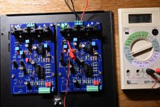
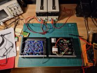
I did some quick DC measurements at both P3 boards using Lab-supply set to -+18VDC.
At opamp I measure V+ = 15.2V and V- = -14.9V at both boards.
Lab supply shows 0.8W from positive and 0.5W from negative. I think 50 mA vs. 30 mA.
CCS shows just above 3mA at one board and just below 3mA at other board (3.1V vs. 3.0V over 1k resistor).
Red D1 led lights. I measure 2mV DC offset at out+.
For JFETs I measure 32 mV over 10R source resistors. So 3.2 mA bias for each JFET.
Over R8 I measure 126mV vs. 121mV. So about 12mA in total.
What did not work was output LED D3. I found out I reversed it on both boards.
I may have been confused at the +sign at PCB and put anode there but I can see that symbol at PCB has a "flat side" and that means Cathode I just verified using google 🙂
So that is the job for today to correct this error and test again.......😡
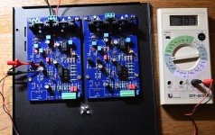
Now light in all LEDs. Was able to reuse the two reserved LEDs.
I also measured voltage over 22R emitter resistors in output circuit. About 0.3V which gives about 14mA bias.
Is that OK?
After a bit of varm-up currents go a bit up.
When UDP3 is connected I will do a bit more burn-in test and measure everything after an hour or so.
Still some work to do before that will happen.
Attachments
I ran into problem once in my BAF2018 line stage build. One channel had an unstable offset and eventually I tracked it down to a 2sk209 which had a fair bit of flux residue around it. Clearing that off resolved the issue.if someone actually gives me example of his own troubles
The flux and thin solder I used was whatever no-name brand the local store had that time so that may have contributed to the problem.
Cheers,
Dennis
Yeah! Thats what I plan to do. The Pearl 3 kit is supposed to arrive Monday. The surface mount parts are the first parts to install. Then toss the bag so I wont know what parts I used... I'll keep the Mouser label. They must be worried about old, corroded parts not taking the solder very well...
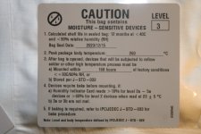
High volume manufacturing of printed circuit boards containing many SMD components, requires that approximately every component must be stored in a low-humidity or zero-humidity environment before pick-and-place and reflow oven soldering. Otherwise the manufacturing yield and the field reliability will be unacceptably low. So lots of SMD parts are shipped and stored in low humidity sealed bags with desiccant packs, especially the high value (high cost) parts.
Preparing to get ready to start soldering U2. I am guessing it can be orientated either way but wanted to check to make sure.
Thanks,
Doug

Thanks,
Doug
NO! You need to orient the faint dot in the corner with the square printed to the left of "U2" on the PCB.
oh, great, thanks @WBS! Wow, that dot is hard to see!! Should have figured there was a reason for the white square dot on the board, nothing superfluous...
Should have figured there was a reason for the white square dot on the board
Alternatively, you could have looked at the manufacturer's datasheet for your integrated circuit called "U2" and checked whether its datasheet pinout is symmetric when rotated 180 degrees. You would have quickly discovered: no it is not, if you rotate the chip incorrectly, its power supplies become reversed (!!) and that would produce an undesirable outcome.
I had good trade for big box of M16, and that's what I'm using now
crikes, M14 are what I use for oil plugs in my car engine. 😳
Kind regards,
Drew
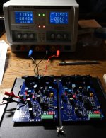
The kit finally arrived on Thursday, and I stuffed and soldered everything this weekend. The power supply is tested OK with load. Will test the Pearl 3 boards later today with the lab power supply. Next step is drilling all the holes in the chassis.
Attachments
Hi,
If I want to make my own PSU, is it useful to "pre regulate" (with 7818/7918 or 7824/7924) before phono boards or a "simple" CRC is enough ?
Damien
If I want to make my own PSU, is it useful to "pre regulate" (with 7818/7918 or 7824/7924) before phono boards or a "simple" CRC is enough ?
Damien
@Abx74
CRC will work perfectly well. Look at the Pearl 2 thread, that was using a CRC. It worked great on P2, and it will also work on P3. Simply get a lower voltage transformer than for P2.
For the Pearl 3 there is the CRCRC offered with the kit. This is inspired by the P2 with extra filtering, snubbers, and an on-board ground break bridge.
There are many other things to try including Mark's umbilical driver PSU, SMPS and a filter board, pre-regulated PSU, Salas, etc.
I'm looking forward to comments from anyone who tries multiple PSU topologies and can describe the differences.
All that said, if I were to pre-regulate... 15+15V transformer (standard for P3) with 18V regs in the PSU would be a good formula. 3V overhead for the P3 regs to work with will be great.
Last edited:
@rhthatcher
Just a quick question while you're handy...
I'm thinking of using your board that came with the kit for another project sourcing parts locally.
The space for the 1W resistors is tiny... most 1W resistors I've found are much larger. Are these gonna get hot? I'm considering mounting these vertically in the centre of the footprints... running "up" the capacitors.
Is there a better approach?
I think we're pulling 50mA per rail x 2 PCB's. Call it 100mA. Neg rail pulls less. But let's call it 100mA as worst case.
Assuming 100mA per rail, and 10R filter resistors, you will see 100mW dissipation for each filter resistor.
P = I^2 * R
1W is oversized. 1/2W will work. 1/4W will also work.
I had the filter resistors rated at 1W for a "FlexReg" supply I did which can go for higher output currents. It can't hurt oversize these a bit.
Alternatively, pick a filter R in the 4-6 Ohm range (4R7) and drop the power dissipation down by roughly half. 1/4W resistor at 40-60mW. It's on easy street.
- Home
- Amplifiers
- Pass Labs
- Pearl 3 Burning Amp 2023