Re Vbe resistor. The transdiode in series with the resistor takes most of the voltage at idle, maybe 0.5V with 0.2V across the resistor. So the resistor needs to be a lower value. It depends on the required mirror ratio and the Is of the transdiode relative to the VAS transistor. My mods have 3.4mA through the Vbe resistor and 8mA through the VAS. The mirror ratio is about 2.4 so you can use the same BJT's for the transdiode as the VAS. Then the resistor is at least 0.2V/3.4mA or 60 ohms. But you need to run it with the transdiodes added to get the best value.
Re models for the LC CCS. It would be nice to run the amp with it modeled to check the temp co's. I don't have the models on hand either, I could get them but it may take time.
Re Rout comparisons. You are comparing this amp to those with (apparently) no output inductor, so use the "nfb" node reading. To compare like-with-like you also need to measure at the same frequency as the other amp value.
BTW Your Ad (difference gain I assume) is -ve when it should be positive. Then use the differential gain 29.5dB (not the SE gain) as the reference gain.
The common mode gain can be measured with "Vin" fed to the inverting input (as well as the noninverting input) then add 29.5dB to the reading (or use two cursors to read the difference).
Thanks for the ESP link.
Since balanced interfacing is not my part of expertise I cannot help you and will have to rely on others to help you clarify what CMRR value is the minimum for a system like yours.
My late 1990 systems have all successfully used ground loop breaking diodes in the mains earthing (except for one unit) and ground break resistors on the inverting input grounding. One system had 5 different stereo amps for auditioning running via a Harmon Kardon preamp/tuner with a turn-table, CD and tape unit and 105dB speakers in a quiet country area, which required hum and hiss to be about 40dB less than typical low sensitivity speakers in a city area. And I got hum and hiss below audibility at 1m. That was 15 years ago and I have never moved into modern DAC's etc so can't advise what's best for your setup.
Re models for the LC CCS. It would be nice to run the amp with it modeled to check the temp co's. I don't have the models on hand either, I could get them but it may take time.
Re Rout comparisons. You are comparing this amp to those with (apparently) no output inductor, so use the "nfb" node reading. To compare like-with-like you also need to measure at the same frequency as the other amp value.
How do you calculate 50 or 80db?
My post #516: I read -50dB up to 1kHz increasing to -20dB at 100kHz. Since the differential gain is 30 or +29.54dB the CMRR is about -80dB up to 1kHz rising to -50dB at 100kHz.
BTW Your Ad (difference gain I assume) is -ve when it should be positive. Then use the differential gain 29.5dB (not the SE gain) as the reference gain.
The common mode gain can be measured with "Vin" fed to the inverting input (as well as the noninverting input) then add 29.5dB to the reading (or use two cursors to read the difference).
Thanks for the ESP link.
Since balanced interfacing is not my part of expertise I cannot help you and will have to rely on others to help you clarify what CMRR value is the minimum for a system like yours.
My late 1990 systems have all successfully used ground loop breaking diodes in the mains earthing (except for one unit) and ground break resistors on the inverting input grounding. One system had 5 different stereo amps for auditioning running via a Harmon Kardon preamp/tuner with a turn-table, CD and tape unit and 105dB speakers in a quiet country area, which required hum and hiss to be about 40dB less than typical low sensitivity speakers in a city area. And I got hum and hiss below audibility at 1m. That was 15 years ago and I have never moved into modern DAC's etc so can't advise what's best for your setup.
I am looking to get -110db s/n out of my amp at 1w output.
I will be real close or better with the power amp set to 20db gain and the tone controls driven by a preamp with a gain of 10. Insertion loss of 17db.
volume pot is driven with a large 8v p-p signal. Headroom 16db 42v p-p
Headroom can be as low as 3db now
AM - ok Fm - ok CD - ok Iphone ok , only turntable or tape inputs benefit from headroom and +16db over 0db is more then can be recorded on either TT or tape.
if you use a resistor and pair of diodes to feed a second low power 1 - 5 w amp gain of 40db and listen for noise
in your speakers using the speaker switch. This way you don't need a super quiet area to test.
Last edited:
The frequency was 20K. Besides, LC's First One Zout declared less than 10mR but with output inductor, don't know the value. He didn't mention if it's on nfb or out. Maybe this is because they use mosfets as op?Re Rout comparisons. You are comparing this amp to those with (apparently) no output inductor, so use the "nfb" node reading. To compare like-with-like you also need to measure at the same frequency as the other amp value.
I measured diff gain with one source to both inputs. Sorry, yes it's positive, 21.9db at 100k. Acm however is much different at both inputs.BTW Your Ad (difference gain I assume) is -ve when it should be positive. Then use the differential gain 29.5dB (not the SE gain) as the reference gain.
The common mode gain can be measured with "Vin" fed to the inverting input (as well as the noninverting input) then add 29.5dB to the reading (or use two cursors to read the difference).
We can raise the CMRR when match the input impedance I guess.
Attachments

Last edited:
....Acm however is much different at both inputs.
Thanks for those screen shots. I can now see how you get your readings.
There are two ways of doing balanced systems: the ground referenced type and the floating type. The ground referenced type with a transformer is where the sender has a center tap and the center tap is grounded. The floating type has no center tap. You are using a floating type of input whereas I have been using the ground referenced bridge driver. ESP Fig 8 Balanced Interfaces top circuit shows the grounded type. The mid and lower ones are balanced types.
Your first run uses the floating form. I used the ground reference type as it can be easily switched from balanced to single ended by changing a jumper position on the inverting input. With this method the balanced gain is double the SE gain.
We need to use the same type of balanced system to compare notes to avoid confusion. Confused?😕 I'll use the floating method from now on.
So delete E1 and connections (In-) including the jumper switch (X1). Hard wire the bottom end of the input source to the inverting input (R16). An AC run will show the differential gain as +23.5dB.
To get the common mode gain wire the inverting input to the top of the signal source and connect the bottom of the signal source to common and read around -50dB at LF. So the CMRR is 23.5+50 or 74dB.
BTW it looks like your second plot (near -0.6dB) has a floating inverting input because the Vin+ label goes no where (since you have deleted E1 in this run). With the inverting input floating there is full Vout to this input so almost unity gain except for some attenuation of the input resistors on the other input). If you connect ground to where the Vin+ is then you get back to a SE input amp. The third plot has a floating noninverting input, but that's OK and you get an inverting SE amp gain of 23.5dB.
Post 520: Ideally CMRR should be infinite, practical values are 95-140db but for DC voltage.
If you are after this then a transformer must be the easiest way. I see Nelson Pass uses a reasonable priced line transformer candidate for the M2 and F6 I think. I doubt you can reach 95dB CMRR with this design. You have made it clear you don't want to use opamps inside your amp.
Probably the optical isolation in a DAC mounted in you power amp enclosure can provide what you want (in principal) but as mentioned last post I don't know what the latest gear actually achieves. Can someone in the know quote actual figures?
Last edited:
Floating signal
Hi AndriyOL,
I did some sims with a floating input source. The attached capture shows how I did it.
When input capacitors are used there is an error -- "floating source". To fix this, add 1G ohms to Rpar (Rt Clk on cap) both input caps. Then you get high THD because the input capacitors have a transient; to fix that make the values 100 and 10 which is Farad's when in reality you use 100u and 10u.
There is a 3rd problem with a floating source -- you can't do a .four on a floating source; to do that you need to use a controlled voltage source as a differential amplifier to shift the voltages to common.
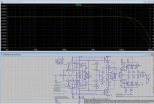
Next I did some temperature stepping to check if adding transdiodes for the VAS idle current. My run showed VAS current was not helped by these diodes and worse the distortion was almost doubled with the diodes. So it appears best to not use these diodes, just use the original 220 ohm b-e resistors.
Note a changed statement: .param d=0 Ta={Temp} Tb={Temp}
This makes all transistors use the same temperature with global stepping, eg .Temp 37 27 . With this statement you can read the change in THD, then probe returns the idle currents for 37C (get 27C current from the original .Temp 27 run).
One further thing. I asked Anthony Holton (Holton Precision Audio) what CMRR is good for power amps and he said 40dB at 1kHz and typically that degrades to 20dB at 10kHz.
If you do decide to use a DAC in the amp then you can have a SE input and a very high CMRR. For SE either revert to the original SE input stage, OR use the Rush input stage in SE mode feeding the inverting input because this gives lower distortion. The Rush input stage has the advantage over the original of being inherently temperature compensated, and a higher input resistance inverting input, which in general offers a low distortion than a noninverting input. BTW There is a thread on input stage distortion recently and I think the advantage of the inverting mode was mentioned.
Hi AndriyOL,
I did some sims with a floating input source. The attached capture shows how I did it.
When input capacitors are used there is an error -- "floating source". To fix this, add 1G ohms to Rpar (Rt Clk on cap) both input caps. Then you get high THD because the input capacitors have a transient; to fix that make the values 100 and 10 which is Farad's when in reality you use 100u and 10u.
There is a 3rd problem with a floating source -- you can't do a .four on a floating source; to do that you need to use a controlled voltage source as a differential amplifier to shift the voltages to common.
Next I did some temperature stepping to check if adding transdiodes for the VAS idle current. My run showed VAS current was not helped by these diodes and worse the distortion was almost doubled with the diodes. So it appears best to not use these diodes, just use the original 220 ohm b-e resistors.
Note a changed statement: .param d=0 Ta={Temp} Tb={Temp}
This makes all transistors use the same temperature with global stepping, eg .Temp 37 27 . With this statement you can read the change in THD, then probe returns the idle currents for 37C (get 27C current from the original .Temp 27 run).
One further thing. I asked Anthony Holton (Holton Precision Audio) what CMRR is good for power amps and he said 40dB at 1kHz and typically that degrades to 20dB at 10kHz.
If you do decide to use a DAC in the amp then you can have a SE input and a very high CMRR. For SE either revert to the original SE input stage, OR use the Rush input stage in SE mode feeding the inverting input because this gives lower distortion. The Rush input stage has the advantage over the original of being inherently temperature compensated, and a higher input resistance inverting input, which in general offers a low distortion than a noninverting input. BTW There is a thread on input stage distortion recently and I think the advantage of the inverting mode was mentioned.
Attachments
Hi Ian,
You did not comment anything about input impedance mismatch, which can be checked by voltage drop at the bases of input transistors. That ought to be a reason of low CMRR. Practical values of CMRR can be found in datasheets of opamps and power amplifier ICs, as I know.
According to formula 20log10*Ad\Acm=CMRR. You just added 23.5bd and 50db.
As for the input transformers, it's known they have limited bandwidth and are overpriced. From my view, they are not an option here.
I don't understand, why do we need to use the DAC in the amp enclosure. DAC input signal source types (I2S, DSD) have very tight limitation in cable length, where it's not a problem at the DAC out.
I think not many people are familiar with balanced amplifier design, especialy in CFA. So, we can't expect some advanced participation here.
Cheers.
I think we have no any ground reffrenece input as we don't use a transformer. Your measurements should be incorrect this way.I have been using the ground referenced bridge driver.
You did not comment anything about input impedance mismatch, which can be checked by voltage drop at the bases of input transistors. That ought to be a reason of low CMRR. Practical values of CMRR can be found in datasheets of opamps and power amplifier ICs, as I know.
According to formula 20log10*Ad\Acm=CMRR. You just added 23.5bd and 50db.
As for the input transformers, it's known they have limited bandwidth and are overpriced. From my view, they are not an option here.
I don't understand, why do we need to use the DAC in the amp enclosure. DAC input signal source types (I2S, DSD) have very tight limitation in cable length, where it's not a problem at the DAC out.
I think not many people are familiar with balanced amplifier design, especialy in CFA. So, we can't expect some advanced participation here.
Cheers.
Last edited:
Hi Ian,
...You did not comment anything about input impedance mismatch, which can be checked by voltage drop at the bases of input transistors. That ought to be a reason of low CMRR. Practical values of CMRR can be found in datasheets of opamps and power amplifier ICs, as I know.
According to formula 20log10*Ad\Acm=CMRR. You just added 23.5bd and 50db.
...Cheers.
I think I see what you mean by CMRR -- you are quoting the value from datasheets of opamps and chip amps (power opmaps). But I have been quoting the CMRR when the opamp is operated in the 4R differential amplifier configuration.
An opamp in a 4R differential amp configuration has a much lower CMRR -- it is determined by the opamps open loop gain and the resistor tolerances and the input source resistance balance. And in practice it is usually the resistor tolerances and not the opamp open loop gain that is the dominant part. With 4R tolerances of 1% you can only expect a CMRR of about 30dB and 50dB with 0.1% resistors.
The input stage current matching is not a significant part of the CMRR for the 4R diff amp -- it is mainly the open loop gain in our simulations since we are using perfectly matched resistors. That's why I haven't commented on them. The input stage current mismatch mostly affects the output offset voltage which will be trimmed out using a trimpot.
As for adding the "23dB" and "50dB" figures you can do that because log(a/b) is the same as log(a) - log (b) and log(b) in this case is -50 (because it is attenuation). So, (minus -50) is +50. So we add the two.
Cheers
What about Dadod's balanced CFA here? Have you considered it? It is proven, has PCB's and gives the ppm's you are after. But not sure what Rout.
The Rush pair as I have used it, converts a CFA into a fully symmetrical VFA.
I note Dadod's is still a true CFA topology. The difference between a CFA and VFA is the low resistance inverting input. Dadod still has one of those.
Rush pairs, as I used them, eliminates the low impedance inverting input and gives two of the same high impedance inputs.
I was wondering whether anyone spotted this? It means your new thread name using "CFA" is strictly speaking a misnomer. Does that matter? I don't think anyone will notice. If they do, maybe call it "a new generation CFA topology" since, as far as I know Rush pairs have not been applied to a monolytic CFA in this way yet -- to have two inputs with the same (high) resistance.
Cheers
Dadod posted the schematic of this amp here before, but it was with buffer, thus VFA as he mentioned in his thread.
Also, it's mosfet, different amp and components.
If there is CFA balanced input with discrete components available there, can we Implement it here in our amp?
Also, it's mosfet, different amp and components.
If there is CFA balanced input with discrete components available there, can we Implement it here in our amp?
What about Dadod's balanced CFA here? Have you considered it? It is proven, has PCB's and gives the ppm's you are after. But not sure what Rout.
<snip>
Hi Ian,
I am afraid AndriyOL is correct, my balanced solution transform CFA to VFA. It uses so called H configuration.
I like your rush cascode solution, and admire your patience here.
The problem I see is influence of the source impedance on the NFB via cold input. In my opinion, solution is additional input buffer before cold input.
BR Damir
Hi Damir,
Isn't it a discrete balanced input without buffer at page 106, post 1057 second schematic?
Isn't it a discrete balanced input without buffer at page 106, post 1057 second schematic?
No, first schematic is unbalanced, to be combined with second schematic to be balanced like in post 1058.
You can find all explanation in the thread.
You can find all explanation in the thread.
You wrote in post 1073 "My CFA amp with balanced inputs does not use additional op amps converters (like instrumentation amplifier) but has built in discrete balanced inputs". This one in post 1058 and LF411 is only buffer ?
Do you know how to make balanced input in the schematic I'm using, even with high impedance input VFA, as you did to use as SE CFA or Bal VFA?
Do you know how to make balanced input in the schematic I'm using, even with high impedance input VFA, as you did to use as SE CFA or Bal VFA?
Last edited:
Thanks for your like.Hi Ian,
I am afraid AndriyOL is correct, my balanced solution transform CFA to VFA. It uses so called H configuration.
I like your rush cascode solution, and admire your patience here.
The problem I see is influence of the source impedance on the NFB via cold input. In my opinion, solution is additional input buffer before cold input.
BR Damir
Sorry, I missed your Q9,Q22 etc making the H bridge.
Attached is AndriyOL's with your H input plus the input buffer.
The first circuit has the buffer shorted to common so just the H bridge noninverting input is fed. It gives 0.1ppm at 1kHz and 15V out.
Next the inverting input via the buffer (noninverting input to common) gives 10ppm.
Then using an ideal buffer (E source) for the inverting input, distortion is back to 0.1ppm. So it's the buffer is causing the relatively high distortion. Have I something wrong? Or is this what theses buffers typically give?
BTW I used subcircuits for the CCS's to reduce drawing clutter. They are cascoded same as your amps (a demo circuit is in the zip).
Attachments
Hi Ian,
For sure that buffer will introduce some distortion, but in your case it does to much in my opinion.
I simulated my balanced 200W "CFA" (simpler output than you use) and THD1k at 15V output is 0.9ppm for hot input only, 1.1ppm for cold input only and 1ppm for balanced input.
BR Damir
For sure that buffer will introduce some distortion, but in your case it does to much in my opinion.
I simulated my balanced 200W "CFA" (simpler output than you use) and THD1k at 15V output is 0.9ppm for hot input only, 1.1ppm for cold input only and 1ppm for balanced input.
BR Damir
Attachments
Thanks for sharing your balanced circuit.
I have changed my buffer to your buffer and get 1.5ppm at 1kHz 15V with balanced input, and 2.2ppm at 20kHz. File attached. BC550C and BC560C give lower distortion in the buffer (than 2SC1845/2SA992 but not sure why).
For 1kHz the amps THD is determined mainly by the buffer THD of 0.9ppm (1V 1k load). At 20kHz the amps THD is determined mainly by the noninverting section and not the buffer.
This looks doable. It uses 14 main BJT's and 12 for CCS's -- a total of 26 just for the input stage.
The Rush version uses 8 main BJT's plus 4 for CCS's -- total of 12 for the input stage but it doesn't give the same true balanced inputs.
Attachments
Last edited:
There is no need for Q12 and Q13.
By the way, in my amp with balanced input and 15V 20kHz THD is 1.2ppm, almost no change in whole audio range.
Maybe you can try my compensation, OITPC.
By the way, in my amp with balanced input and 15V 20kHz THD is 1.2ppm, almost no change in whole audio range.
Maybe you can try my compensation, OITPC.
Last edited:
Revised balanced Rush input stage
Thanks for spotting that.
I have further modified your H stage buffer using Rush pairs which reduces transistor count.

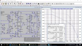
Then I also added 2 buffers. Why is this necessary?😕 I found the noninverting input needs a buffer to match the gain of the two inputs to get a high CMRR. The noninverting input needs attenuating with a 1k and 15k voltage divider, hence the need for the 2nd noninverting buffer so the two inputs also have the same high input resistance. THD is around 0.5ppm at 1kHz 15V, and 1.6ppm 20kHz.
Without this 2nd buffer and attenuation on the noninverting input the CMRR is quite low, around -20dB; it is from the unmatched gain difference of the two inputs (without the noninverting attenuator).
Recall a noninverting opamp has a gain of 1+Rf/Ra and the inverting input opamp has a gain of Rf/Ra, or a gain of 1 different. In a 4R diff. amp we add two resistors to the noninvering input to reduce the gain from 1+Rf/Ra to Rf/Ra, which can be done with values "Ra" and "Rf" for the divider.
This circuit is still basically the same as my original Rush "SSAHP" (eg Post 509) but with 2 input buffers, also I now use your cascoded CCS's (hopefully for a lower temp co to reduce output voltage drift with temperature).
To reduce the transistor count use 10k resistors instead of CCS's for the buffers; 8 less tr's. THD increases at 1kHz to 1ppm and 20kHz falls slightly to 1.4ppm and the CMRR is not impaired (see below 1kHz -50dB, so net CMRR is 70dB at 1kHz).

So overall I'd say it's OK here to omit the CCS's for the buffers.
- - - -
Re Using alternative compensation like your OITPC -- you can try adding it to this latest version. I am hoping AndriyOL is picking up LTspice so he can take on any changes and build his version as the master version.
@ AndryOL. What do you think of these changes?
BTW the input stage is now VFA type (like Dadod's balanced one) -- is that an issue for you?
Thanks for spotting that.
I have further modified your H stage buffer using Rush pairs which reduces transistor count.
Then I also added 2 buffers. Why is this necessary?😕 I found the noninverting input needs a buffer to match the gain of the two inputs to get a high CMRR. The noninverting input needs attenuating with a 1k and 15k voltage divider, hence the need for the 2nd noninverting buffer so the two inputs also have the same high input resistance. THD is around 0.5ppm at 1kHz 15V, and 1.6ppm 20kHz.
Without this 2nd buffer and attenuation on the noninverting input the CMRR is quite low, around -20dB; it is from the unmatched gain difference of the two inputs (without the noninverting attenuator).
Recall a noninverting opamp has a gain of 1+Rf/Ra and the inverting input opamp has a gain of Rf/Ra, or a gain of 1 different. In a 4R diff. amp we add two resistors to the noninvering input to reduce the gain from 1+Rf/Ra to Rf/Ra, which can be done with values "Ra" and "Rf" for the divider.
This circuit is still basically the same as my original Rush "SSAHP" (eg Post 509) but with 2 input buffers, also I now use your cascoded CCS's (hopefully for a lower temp co to reduce output voltage drift with temperature).
To reduce the transistor count use 10k resistors instead of CCS's for the buffers; 8 less tr's. THD increases at 1kHz to 1ppm and 20kHz falls slightly to 1.4ppm and the CMRR is not impaired (see below 1kHz -50dB, so net CMRR is 70dB at 1kHz).
So overall I'd say it's OK here to omit the CCS's for the buffers.
- - - -
Re Using alternative compensation like your OITPC -- you can try adding it to this latest version. I am hoping AndriyOL is picking up LTspice so he can take on any changes and build his version as the master version.
@ AndryOL. What do you think of these changes?
BTW the input stage is now VFA type (like Dadod's balanced one) -- is that an issue for you?
Attachments
I simulated Loop Gain with the Tian probe and the result is quite suboptimal.
PM is 20 degree only and GM is 7 dB.
I like your balance approach with the Rush cascodes and will tray my amp simulation with it.
By the way I don't think that the gain differences between hot and cold inputs are important for good CMRR but equal input impedances.
I my amp the cold input gain is hot input gain-1 and I don't equalize it.
Best wishes, Damir
Attachments
- Home
- Amplifiers
- Solid State
- One of the Top Solid-State CFA amp design