Shouldn't those 0R22 resistors be placed at the emitters of your output devices? Or shouldn't the output devices be swapped (C5200 to the positive, A1943 to the negative rail), each one given it's own emitter balancing resistor?
Best regards!
Thanks. Yes, your thinking is sound about the resistors being moved to the emitters. Essentially, I have 0.055 ohms for each emitter of each compound pair: 0.22 / 4 for four output pairs.
For pure resistive load, the power of interest is at about 0.95A per pair for 8 ohms (for 150 W configuration). this translates to about 0.2V over 0.22 ohms. Not really significant enough, in my opinion. For 4 ohms use, it may be useful to move them. I've never experienced BJTs being that far off from each other ever. So balancing emitters is safe, but safer is to just check the transistors first, especially for compound pairs.
In my experience, adding the emitter resistors (as shown) has no real benefit. Theoretically, the best THD performance I have seen comes from when there is no emitter resistor. Basically, the 0.22 ohm resistors create a PCB layout jumper. 😀
I believe that adding emitter resistors changes the non-linearity of the emitter PN junction, which then becomes more linear. So the more current you output, the larger the emitter voltage drop becomes, making the output more dependent on the emitter resistance. The feedback has to then compensate for this. I think for the alternative configuration I've shown, this simply adds a little more strain to the drivers, because they need to drive more current to meet the output emitter resistance changes. I believe this linearity of the emitter resistance is the reason for higher THD with higher output resistance. I could be wrong. Sure, emitter resistors can ensure you get better current matching with device variance, but I don't think it's much to worry about.
As far as I know, the idea is to create more emitter resistance as the output current increases due to device heating, and thus smaller Vbe, but the heating of devices is far far slower than the changes in output current (thank goodness). Either way, the compound pair is unbelievably thermally stable, provided you don't drive the drivers too hard, and you thermally connect the bias control and the drivers.
Oh, and one more important thing - I would definitely say that in addition to matching your transistors somewhat, I would put all the output transistors on one heatsink, or at least all the NPN's of one amplifier on one heatsink, and all the PNP's on one of their own. This at least helps the emitter resistance to remain fairly relative from device to device.
The alternative is as I've shown attached.
Ok, so all that said, if you end up with transistors that really aren't that well matched, emitter resistors are a good thing. So, with that in mind, I think the best configuration is the second attached image.
Thanks for the insight! It made me think a little more about the output.
Attachments
I've never experienced BJTs being that far off from each other ever. So balancing emitters is safe, but safer is to just check the transistors first, especially for compound pairs.
In my experience, adding the emitter resistors (as shown) has no real benefit.
Sorry, but I don't verify this statement. Even if we manage to find two devices that exactly do match by any parameter, which we most certainly don't, we will observe that these won't heat up equally, just from sitting at different spots of the common heatsink, thus at least one parameter will drift.
Omitting balancing resistors is solely allowed for MOSFETs in switch mode.
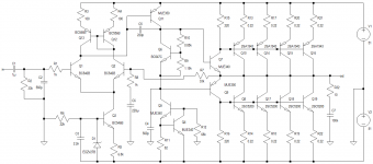
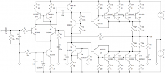
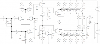
This reminds me of the 1970ies ES-707 amplifier by German manufacturer K+H. The power stages clearly resemble a design from the RCA Transistor Manual, to which the engineers simply added one more pair of output transistors (BDY56 in this case). Strangely, they put 0R22 'balancing resistors' in the collector leads of the negative rail's devices (and used a B40C5000 bridge for rectifying 63Vac, btw...).
Your new schematics are puzzling me as well. If you rotate the bias trimpot especially in the first drawing, you'll initially see no idle current at all, them a sudden jump to zillions of Amperes, only limited by the PSU's internal resistance, the power devices (which most certainly will fail) and the 0R22 resistors.
Best regards!
Last edited:
Sorry, but I don't verify this statement. Even if we manage to find two devices that exactly do match by any parameter, which we most certainly don't, we will observe that these won't heat up equally, just from sitting at different spots of the common heatsink, thus at least one parameter will drift.
Thanks, you're right. Like I said, I could be wrong. On inspection, the balancing resistors mitigate potential mismatches, and it's a good idea.
Your new schematics are puzzling me as well. If you rotate the bias trimpot especially in the first drawing, you'll initially see no idle current at all, them a sudden jump to zillions of Amperes, only limited by the PSU's internal resistance, the power devices (which most certainly will fail) and the 0R22 resistors.
Yes, the first one is difficult to set up. I've done it, and it is possible, but for certain conditions, it actually isn't possible to set up.
The second one is easier; I've done a similar setup with two pairs per amp with 0.22 ohm balancing resistors, and 0.1 ohm output resistors, and I set it up with a single-turn pot. I must say it wasn't easy at all! 😀 But here it's a 10-turn pot, and with these values, I haven't had issues or drift.
I guess there's nothing wrong with increasing the output resistors. Say to 0.68 ohms each minimum? I'd say up to 1 ohm each should be fine.
Thanks for the insight! 🙂
I thought the best advantage of emitter resistors on the output transistors is eliminating thermal runaway. As Vbe sags with heat, the voltage drop on the emitter resistor increases. That reduces the gain in base current with heat.
Peavey PV series for emitter resistors uses 0.5 ohms and AX6 use 0.51 ohms, I'm sticking with that. Dynaco ST120 didn't have one on the negative transistor and kept blowing transistors.
My matching transistor procedure is pretty stone age anyway. put transistor on little heat sink, 12 dc to collector through 10 ohms, same to base through 100 ohms, run a half minute measure Vce. Mark with sharpie. Outlier values go to another project. I had 20 transistors at .13 and .14 v last project and four at 0.11-.12. Used the 20.
Emitter resistors don't cut output power by hardly any decibels at all , since the ear is logrithmic.
I thought the best advantage of emitter resistors on the output transistors is eliminating thermal runaway. As Vbe sags with heat, the voltage drop on the emitter resistor increases. Peavey PV series uses 0.5 ohms and AX6 use 0.51 ohms, I'm sticking with that. My matching transistor procedure is pretty stone age anyway. put transistor on little heat sink, 12 dc to collector through 10 ohms, same to base through 100 ohms, run a half minute measure Vce. Mark with sharpie. Outlier values go to another project. I had 20 transistors at .13 and .14 v last project and four at 0.11-.12. Used the 20.
Emitter resistors don't cut output power by hardly any decibels at all , since the ear is logrithmic.
Absolutely, thanks!
Yes, emitter resistors (R24 - R27 in my last schematic) must not be omitted, except if you're planning a class B amplifier with lots of crossover distortion. Leaving them off will be asking for trouble, but at least the compound pairs are very stable thermally.
The 0.1's match the output transistors sufficiently (can probably be increased to 0.22 ohms), and the output resistors provide some local feedback (not sure how this affects things), and allow a more stable setup. The difference with 4 0.68's rather than 0.22's is 145 W / 8, 275 W / 4 vs 142 W / 8, 260 W / 4. Not much difference at all.
Why don't you go with emitter follower power devices?
Best regards!
This is an emitter follower output. Do you mean Darlington configuration?
I prefer the thermal stability and PCB layout of the compound pairs. I also like the extra 0.6 V output... 😀
I use a Darlington output configuration on my guitar amplifiers. It's a 50W amp, and it performs incredibly well. It's also an easy amp to build and set up. I have nothing against the Darlington configuration.
Oh, please note, it's not MJE340/50, it's 2SC1837/2SA4793.
you have a common emitter output.This is an emitter follower output.
Darlington is an integrated two device component that brings out three leads and forms a dual emitter follower (common collector)Do you mean Darlington configuration?
the common emitter topology that you are proposing is reputed to be much more intolerant of poor PCB layout/component inductances/inadequate compensation.I prefer the thermal stability and PCB layout of the compound pairs. I also like the extra 0.6 V output... 😀
This fits with what little I know about the two topologies.I use a Darlington output configuration on my guitar amplifiers. It's a 50W amp, and it performs incredibly well. It's also an easy amp to build and set up. I have nothing against the Darlington configuration............
Darlington is an integrated two device component that brings out three leads ...
I think we should agree with Mrcloc that there are discrete darlingtons, made up from two transistors of the same polarity and one or two resistors, and even complemetary darlingtons, aka Sziklai pairs, as well.
Monolithic, three-legged darlingtons came to the market well after this principle's invention.
Best regards!
you have a common emitter output.
Darlington is an integrated two device component that brings out three leads and forms a dual emitter follower (common collector)
the common emitter topology that you are proposing is reputed to be much more intolerant of poor PCB layout/component inductances/inadequate compensation.
This fits with what little I know about the two topologies.
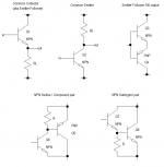
Let's be clear about what's called what. That's the first thing (see attached image).
Basically, you have an "emitter follower" output if you have something which can be simplified down to what I've shown as an emitter follower AB output, obviously.
If you break down the NPN of the AB output shown (assume it is biased), then there are two common configurations: Sziklai / compound, which can be seen as a common emitter, and a Darlington, which can be seen as a common collector.
If there is an output stage that (simplified) doesn't look like the emitter follower AB output I've shown, I don't know about it. Thus, I refer (in my answer to Kay Pirinha) to the broken-down structures, ie. Sziklai vs Darlington.
Darlington configuration refers to the configuration of cascading 2 (or more) BJTs of the same polarity, not the monolithic device (TIP127/147/ et al.), which would be referred to as a (singular) "Darlington transistor".
In terms of stability, you can most certainly have a common collector (gain of 1) oscillate. Similarly, you can easily have a common emitter (gain of >1) oscillate. Sure, the compound pair is less tolerant of certain factors than a Darlington configuration, but the compound pair is better thermally, and this is something which cannot be predicted as easily as oscillations in the real world. With oscillations, solve it for one, solve it for all (generally). But you have no control over how a user will use the amplifier, in terms of the cabinet it's in, the other components it is near, etc. There is far more to it that this. I'm not nearly as experienced as many on these forums, but in my 14 years of amplifier building, I've learned a thing or two.
Attachments
The current mirror in the LTP does a lot for reducing noise on the output, but I find it increases the O/L gain significantly, and this is not necessarily an advantage. I'm not sure how others feel about this, but I would just leave it out, connect the collector of Q2 to Vcc, and connect the collector of Q1 to Vcc via a 330 ohm resistor. This is easier, and the major place where noise (hum) is reduced is the current source on the tail of the LTP. The O/L gain is still very large.
I have started to build this one now. I've made one or two modifications, but the circuit remains much the same. I'm using BC546 throughout for small signal and low-power current source drivers. These were selected for ideal capabilities, and comparably low noise. I'm using MJE15030 and MJE15031 as the class A transistor and its current source, as well as the drivers. They do a reliable 100 Hfe in the entire range they'll be used in. I'm using 5 pairs of 2SA1943/2SC5200 on the output, with 0.15 ohm emitter resistors to balance them. All 10 output transistors will be mounted on a 0.45K/W heatsink (it's huge), with thermal switches on each heatsink, which will switch on a fan if the heatsink temperature reaches 95C. The circuit was changed slightly to accommodate +-57Vdc supply.
This amplifier will do around 330W into 4 ohms, and 180W into 8. I will post successes / failures as I build. I will also post a schematic sometime. Components are being delivered now, and the last are due to arrive on March 20 the latest. I'm excited about this one.
This amplifier will do around 330W into 4 ohms, and 180W into 8. I will post successes / failures as I build. I will also post a schematic sometime. Components are being delivered now, and the last are due to arrive on March 20 the latest. I'm excited about this one.
5pairs of 1943/5200 have a reliable maximum output of around 250W when on a sensible heatsink temperature feeding a severe reactance speaker.
If you allow your hetasink to go as high as 95degrees C, then your max output will be lower than 250W.
180W into 8ohms is a reasonable target.
330W into 4ohms is risking disaster.
I'd suggest you fit a much lower sink temp switch, maybe 50, or 70 degrees C
Don't use a crossovered 4ohms speaker.
6ohms crossovered, or a less reactive single driver of 4ohms rating would be more suitable.
5pairs of 1943/5200 have a reliable maximum output of around 250W when on a sensible heatsink temperature feeding a severe reactance speaker.
If you allow your hetasink to go as high as 95degrees C, then your max output will be lower than 250W.
180W into 8ohms is a reasonable target.
330W into 4ohms is risking disaster.
I'd suggest you fit a much lower sink temp switch, maybe 50, or 70 degrees C
Don't use a crossovered 4ohms speaker.
6ohms crossovered, or a less reactive single driver of 4ohms rating would be more suitable.
Thank you for that input. I've done extensive calculations. Here are my findings (and why I use 5 output pairs). Consider a resistive load of 4 ohms:
Peak output power of one transistor = 36W.
At a sink temperature of 95C, the transistors will be at around 105C.
These two values are well below the derating curve.
Then, the point closest to the SOA curve is at 850mA and 37V and that's miles below the SOA curve. Even with derating, I'm well within limits.
Furthermore, the maximum sink temperature for a resistive 4 ohm load at 40C ambient is 94C. This is also for the worst case scenario sine wave.
To stress the transistors, the load will need to be very difficult, the output must sustain worst-case for a LONG time, and the amplifier needs to be in direct sunlight on a summer's day, and then a full peak output voltage must occur at a frequency which the speaker shifts >90 degrees.
If the heatsink manages to reach 95C, the fan will turn on to rapidly cool it.
A few other considerations. The heatsinks are theoretically 0.4 K/W; I've been overly conservative in my estimated value. I have also assumed the airflow will remain the same, even if the sink rises 50C above ambient. My fans provide about 530 LFM, which will drop the heatsink K/W to 0.2.
So those are my calculations / considerations. I'll see how it goes when I've built it. I expect a music signal to sustain an average of 60 or 80 W for a 4 ohm load, and I suspect the heatsinks won't heat up much, even under sustained heavy use. I could be completely wrong, but I've also tested my two 0.6 K/W heatsinks driving a sustained heavy load for a long time, and they barely heat up. This is for a 130 W amplifier.
For some extra reference, here's Rotel's RB1590, which supposedly does 350 into 8ohm (per channel). By the looks of things, they use two output pairs, and the heatsinks can't be better than 0.3 K/W. For now, I'm going to say I'm good.
Have you read David Eather and how to determine the SOAR for a reactive load?
Jan Didden has a similar SOAR prediction based on a quite different method.
Jan Didden has a similar SOAR prediction based on a quite different method.
Have you read David Eather and how to determine the SOAR for a reactive load?
Jan Didden has a similar SOAR prediction based on a quite different method.
Let's use a formula I've seen you use:
Power = 330W, use DF = 5, then total device power needs to be 1650.
1650 / 10 = 165W.
So I'm 10% off, according to your formula.
I only look at the DC SOA. At 90 degrees, the current is 1.8A and the voltage is 36V. That's well below the DC SOA.
I've done a calculation for derating and extended hard use under normal circumstances, and the design points are well below the maximums. I'm well in the safe operating regions.
I've also simulated a reactive load, and the simulation also doesn't come close to maximum ratings.
if you look at the higher voltage SOA of 1943/5200 you will find that they do not tolerate high current and high Vce simultaneously as well as other devices of similar power.
I have suggested that the BJT de-rating factor for BJTs should be around 5 to 6.
That is why I suggested you limit your 5pair stage to 6ohms or higher speaker loads. Unless you are driving a low reactance single driver, where you can probably use a 4ohms directly driven speaker.
1943/5200 need the upper end, if you require reliability into severe reactance loads.
Read David Eather. See the effect of 45degrees and 60degrees of reactance on the IV
It is MUCH worse, than for resistive loads.
- Status
- Not open for further replies.
- Home
- Amplifiers
- Solid State
- New design 135W 8, 270W 4