Hi Frans
What is the purpose of the smaller case to the left ? The one with dedicated psu ?
At the back there is an copper box with ADC (left/back) and metal box with mains connector and filter (right/back). Front left meta; box PSU for the ADC next big copper box RIAA preamp next metal box PSU for RIAA preamp.
In the RIAA preamp there are 3 sections, first whider section is secondary PSU, middle small sections tertiary PSU and large sections RIAA preamp.
The primary PSU for the RIAA preamp in the big metal box (right). The copper tube is used to transport mains power to the ADC PSU.
Balanced RIAA preamp | Flickr - Photo Sharing!
Balanced RIAA preamp | Flickr - Photo Sharing!
I found this in the big mail order catalog of Manufaktum. They belong to the huge OTTO
group. Interesting how they talk about mechanically stored music.
Sorry, this is in German.
Stereophonie - Manufactum
group. Interesting how they talk about mechanically stored music.
Sorry, this is in German.
Stereophonie - Manufactum

I own a Rega P3 and if partnered with a good MC and good phonos, is capable of outstanding results. I guess the arm is really important in this success.
Attachments
Last edited:
Yes, the Regas are the budged champions. I really like the arm and some of the modifications.
Thanks for translating. I find it really interesting that a super commercial outfit like that goes into vinyl. I do not think that they praise products that they can not sell.
Thanks for translating. I find it really interesting that a super commercial outfit like that goes into vinyl. I do not think that they praise products that they can not sell.
Don't you hate the anti skating slider, the non VTA, and the ground blending in the wiring on a Rega? I do.😀
Wow I have to do with a TD160 and SME3009-MKII with Sure V15X MR
Flickr: Search F.d.W.'s photostream
Flickr: Search F.d.W.'s photostream
I heard very good things about the Ortofon MMs. As far as i know the 540 range is not available in Germany. Here it is the Vinyl Master series that is supposed to be tuned different. I will check that out. I really would like to have a good MM that is better then the AT95E.
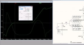
Have been looking at the input impedance, but not really sure how to set up a good measurement for this, the generator input impedance may play a role in the equation...
but according to this the impedance is app 2Kohm,,,to 100 KHz then slowly decreasing.. (input voltage is 1 V and The current is monitored)
Also I have a little problem with the internal shunt, as there's no absolute reference it varies with the input-currents from the floating JFET current sources, could be a LED string reference combined with the JFET CCS's is a good solution, here I have degeneration problems as the CCS must pass app 15mA to maintain a 10 V cascode spread.
Attachments
Did you get good matches, when measuring BC337/BC327-40? Or should one better try to match BC327-40 with BC337-25?
Rüdiger
Rüdiger
MiiB,
if you could provide me with the LT-Spice file I would look it up. Otherwise, it's though for me to see why we'd need 15mA for a Cascode reference? Same for the floating voltage issue.
Rüdiger
EDIT: yes, the voltage varies a bit when the CS fet warms. But since it's independent from both PSU noise and signal interference I doubt it matters. We should run the fet at zero tempco. I did not bother with in my phono pre, and the offset is stable around 0mV
Rüdiger
Last edited:
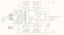
Rudiger,, I use 10 of those mA for the circuit, 2,5 mA for each input transistor, the rest is for the shunt to work....Attached here is a version where all the deratings are OK, the maximun is 100 mW/device
A JFET Current push, will dissipate app 350 mW, and that just too much for the poor device.. and for tha JFET CCS in the mirror for the buffer it was 600 mW, so these are now changed to simple Resistance elements, I do feel that it no a degradation as we already have a very-good shunt regulated supply..
I have changed the internal mirror shunt to a CCS'ed LED refrence, at app 12 V
I have inserted a cascode in the buffer current souce, to reduce power dissipation in the Lower device....
Attachments
Last edited: