No sane manufacturer will wire bond high current pins with 25u gold wires. That’s what aluminum wire bonding is for. Check a power device of your choice. You will note multiple aluminum wires to the emitter/source pad(s).
High current pins? I thought this discussion was about an audio DAC. Those usually don't draw more than a few hundreds of milliamperes.
If what you measure is correct, this men’s all AVCC pads are not shorted by the metallization layers, but through diffusions.
Not necessarily, when both pins are double-bonded with 4 mm long, 25 um thick gold, that already gives you 0.2 ohm. Besides, the on-chip metallization also has resistance, usually a few tens to a few hundreds of milliohms per square.
It would take some effort to make a 0.2 ohm connection in diffusion layers. Highly doped and silicided layers typically have a sheet resistance of the order of 15 ohm per square, so you would need a connection that's 75 times as wide as it is long. If you want such a low-ohmic on-chip connection, it makes more sense to use some thick metal layer. If the intention was to keep the AVCCs separated, then obviously something must have gone wrong when the resistance is only 0.2 ohm.
I doubt the measurement is correct or there is something being missed. ESS is presumably not stupid enough to bond out 4 pins per AVCC input only to achieve 0.2 Ohms. In a high resolution instrumentation-grade converter I am not sure 200 mOhms would be acceptable for a voltage reference input, and this one draws more current than typical DAC or ADC reference inputs.
When the resistance between two AVCC pins is 0.2 ohm and they are internally connected by huge thick-layer metal grids, four pins together give you a bit over 0.025 ohm between the external and the internal supply: 0.1 ohm in series with 0.1 ohm versus four times 0.1 ohm in parallel.
Extrapolating microwave circuitry behavior to audio DAC frequencies, nice try. Why don't you just match all clock lines and be done with it. Hint, it is not needed since the clock trace lengths are always (except pathological implementations) much, much shorter than the clock wave length/16.
Mind you, what matters is the transition time rather than the clock period time.
Mind you, what matters is the transition time rather than the clock period time.
Yes, but I have seen products with GHz RF on short uncontrolled impedance antenna feeds and they work well enough to not significantly harm performance and still pass carrier compliance testing. There is simply no need for a transmission line structure for a short single-ended LVCMOS clock trace. They are never properly terminated in practice and almost always include the estimated 22-47 ohm series resistor at the driving end.
It is not a proper termination. It is almost exclusively used in the real world with unknown source Z values and uncontrolled trace impedance. Further, the output impedance of CMOS can change significantly with logic level. I have never seen it used where an actual terminated transmission line is required and signal integrity is important.
Last edited:
What's improper about it? It's somewhat inaccurate and it allows one reflection at the far end, but with termination on both sides you would halve the signal and not be LVCMOS compatible anymore.
What's improper about it? It's somewhat inaccurate and it allows one reflection at the far end, but with termination on both sides you would halve the signal and not be LVCMOS compatible anymore.
I’d consider it more damping, than termination in most cases as it’s applied. Sorry for the ninja edit above.
Last edited:
For your information, I started writing post #269 when post #268 consisted of only one line. I think we pretty much agree.
For your information, I started writing post #269 when post #268 consisted of only one line. I think we pretty much agree.
I see, yes.
When the resistance between two AVCC pins is 0.2 ohm and they are internally connected by huge thick-layer metal grids, four pins together give you a bit over 0.025 ohm between the external and the internal supply: 0.1 ohm in series with 0.1 ohm versus four times 0.1 ohm in parallel.
I misread Peufeu’s test conditions and assumed the equivalent resistance was 0.2 ohms, not just between two of the four pins. Seems more reasonable with four.
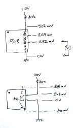
I dug out that 9018 test board. It has 1R resistors in all the power supplies to measure current. Took them out, which gives direct access to AVCC pins for a Kelvin resistance measurement.

Measured resistance is sum of bondwires + internal chip metallization so it is not exactly obvious what the share of each of those in the total resistance is... but the values are coherent with a longer path from top to bottom than between the two pins on the side.
On top pic, current flows between top and bottom pins, the two side pins act as kelvin sense, so there's 15 mOhm on-chip resistance between them. They're probably connected to very close pads on the chip.
On bottom picture, that would leave about 0.12 ohm per bondwire for the side pins (nitpickers will substract half of the previous 15 mOhm to that). The two pins on top and bottom act like kelvin sense and confirm this.
Top and bottom pins seem to have a bit higher resistance.
Last edited:
Not sure what you mean by “current drawn by one channel shows up on all the AVCC pins”, perhaps you mean voltage?
I mean one channel was playing a sine wave with the output open (no IV connected to it) so it drew variable AVCC current.
There was a 1R resistor between each AVCC pin and the actual AVCC power supply.
I measured voltage on each resistor to get current flowing into each AVCC pin.
Since they're all connected internally, it is no surprise that the AVCC current for one channel is spread between all AVCC pins. It's probably not spread exactly between the pins since the internal resistance path between each DAC and each pin is different, but I didn't see a point to dig further, since in a proper implementation (ie, balanced IV) AVCC current is constant anyway.
Extrapolating microwave circuitry behavior to audio DAC frequencies, nice try. Why don't you just match all clock lines and be done with it. Hint, it is not needed since the clock trace lengths are always (except pathological implementations) much, much shorter than the clock wave length/16. Extreme example: 100MHz clock, assume x10 to provide good bandwidth, 1GHz has 30cm wave length, any PCB trace running an 100MHz clock under 2cm will exhibit very weak transmission line characteristics.
But the OP asked about analog signal at the output, which is well under 100KHz, so your answer is pure FUD (again). You made the following extrapolations: Need to keep an 100MHz clock timing and integrity->same for analog audio outputs->therefore analog audio outputs are subject of the same constraints as the clock lines. Even if this would be true (which, for all audio purposes, it is not, not even close) there are simple methods to separate the analog and digital grounds, like for ADC/DACs in the Gbit/sec range, ex. for SDRs.
Yes, I know, "some people feel has an effect on SQ", always your ending FUD statement.
I'm confused too, then that pin should be DVCC instead of AVCC right?
I'm confused too, then that pin should be DVCC instead of AVCC right?
What pin?
If one looks at some of the dac projects around this forum it should be obvious that people are running clock wires, not even traces, much longer than 2CM. Many of those people may have been misinformed to the effect that 'it doesn't matter for audio.'
As to understanding of what does matter for audio, everyone can decide what they think for themselves:
https://www.diyaudio.com/forums/equ...trumentation-applications-45.html#post6524953
...Post #441
As to the calling of FUD:
Choosing of best sounding OP AMPs for the lowest possible THD+N -really the best Way? ...Post #452
Last edited:
High current pins? I thought this discussion was about an audio DAC. Those usually don't draw more than a few hundreds of milliamperes.
Discussion is way OT, but know that a 25um gold bonding wire melts (acts as a fuse) at about 0.5A (or less, there are many factors involved). Not a good idea to use it, even for "a few hundreds of milliamperes". To add insult to injury, bad things may start to happen at current densities much before the bond wire melts (and that's another OT discussion, about electromigration).
Aluminum bond wires melt at lower current densities, but can be made (economically) much thicker (and with lower resistivity).
Regarding the sheet resistance of diffused layers, not sure where you got the "15 ohm per square" value for diffused layers. In fact, if this would be some sort of limit, bipolar transistors could not be built 😀. The minimum sheet resistivity is orders of magnitude lower, check out the tables in https://nvlpubs.nist.gov/nistpubs/Legacy/SP/nbsspecialpublication400-64.pdf
Mind you, what matters is the transition time rather than the clock period time.
Of course, but if the clock distribution network doesn't have enough bandwidth, the rise/fall times are affected. You would of course know that, the rise/fall times and jitter are directly related. This is to say that the clock distribution network may add significant additive jitter to the original clock.
Not that it really matters in practice, this is in a nutshell my entire beef with the jiteratti gang; they are contemplating a few fs jitter clock, suspend the oscillator by rubber bands to avoid earth crust vibration effects, feed it in the DAC (or whatever) chip, where the on chip clock distribution adds enough jitter to justify a 50 cents quartz crystal clock source.
If one looks at some of the dac projects around this forum it should be obvious that people are running clock wires, not even traces, much longer than 2CM. Many of those people may have been misinformed to the effect that 'it doesn't matter for audio.'
The practices of a bunch of people that have no idea what they are doing is not relevant. When I see a rat's nest of wires connecting a bunch of eBay / Alibaba PCBs and the odd evaluation board I know it's already a waste of time.
- Home
- Source & Line
- Digital Line Level
- Low noise regulator for DAC & clock