Higher Vref will result in a little higher dac output voltage. Its a mulitiplier, so in terms of dB a few tenths of a volt may not much in the way of perceived volume level.
This hardly matters if one is using the digital attenuation of the DAC chip no? Whatever gains or losses in the output range here are somewhat irrelevant.
What you are describing regarding the current drawn from Vref makes me think that logically the lower the current the lower the low level voltage fluctuations. Since the Vref current draw is less for 3.3V Vref in the datasheet, wouldn't that make for a lower THD+N value? Still the datasheet states a higher noise figure for 3.3V Vref. True that it's also with 3.3VACC so that might have an effect. But the way I understood it, VACC is only powering the output driver, it's something like the power supply for the output opamps. So that would set the final output capability of the DAC. Let's say you have a 5V Vref and 3.3V AVCC, when you get past 3.3V swing you hit the rails on the AVCC, even if the DAC can use 5/(2^32)V steps. So then I understand that lower Vref means lower dynamic range, but why higher THD+N?
Using the digital attenuation means that very very few people would usually have a 2-3V swing if going from DAC directly to your average amp+speaker combo dB wise. Wouldn't theoretically make sense that a lower Vref would translate into lower effects that you are describing? Also es9018 has a lower Vref and around 3Vpp output.
Distortion arises because the current draw of the Vref load is not constant. When more current is drawn the regulator must respond by trying to hold the voltage constant. Since its error amplifier has finite gain, the voltage will never be perfectly constant. Also, since the error amplifier will have some nonlinearity, its response in trying to hold the voltage constant will not be perfectly proportional to the current draw. Thus drawing a sine wave of current will result in some very low level voltage fluxuations at harmonics of the current sine waveform.
Even when the regulator and its decoupling don't distort at all, you can still get distortion from a nonzero reference impedance and data-dependent reference current: undistorted signal at the reference times undistorted signal at the digital input produces second order distortion at the output.
Besides, normally a DAC chip designer would try to compensate out the data dependence of the reference current and imperfections of this compensation cause a remaining data dependence that does not necessarily follow a straight line. That is, the reference current variations may already be distorted.
I would not use the digital attenuation in a dac chip if the dac chip supports DSD bypass. The issue there is that DSD may have to be turned into PCM to control the volume inside the dac chip. There will necessarily be a loss of sound quality in that case. Since some dacs sound their best in DSD mode, there can be a significant cost to using the internal volume control.
Regarding THD+N, it is a largely useless metric as it cannot come close to predicting how a piece of audio equipment will sound. Some people like the sound of low level, low order HD (2nd and or 3rd). Higher order harmonics are much more perceptually objectionable. Earl Geddes, a speaker designer and hearing researcher proposed a new metric that would more closely correlate with how humans hear. Unfortunately, it never caught on. THD+N was originally used mostly because it was so easy to measure. Just feed in a sine wave, run the output through a notch filter, and whatever is left must be THD+N (those were the very old days). Unfortunately, the metric remains popular with manufacturers. Many don't want to measure/publish more than the minimum they can get away with.
Regarding Vref (or AVCC for ESS dacs), the reason for using an opamp buffer and why it often sounds better than other alternatives is simply because they are very low distortion amplifiers. AD797 remains a very, very good one. If they didn't sound better to dac designers who bother to do listening tests, nobody would bother to go the trouble.
One more thing: Not all distortion is easy to measure. Some may look more like noise when using common measurement techniques since there is an implicit assumption that distortion will remain stationary over the time frame in which it is being measured. That is not always the case with DACs IME. Perhaps not surprising considering that there is RF (deterministic RF and RF band noise) radiating from the dac chip and significantly mixed in with the analog audio output of the dac. It can have peculiar sounding effects in opamps for reasons that may vary from opamp to opamp. It is known that forward biased PN junctions can demodulate RF and the resulting voltage can shift internal bias levels inside an opamp. It has also be suggested that high levels of RF noise may cause slewing distortion in output stage opamps. Sometimes such effects show up weakly on an FFT yet remain quite audible. In that case part of the energy of the distortion (or of noise that sounds like distortion when mixed in with audio) may appear as a small broad shift of the FFT noise floor. Of course, in SD dacs the noise floor is modulated by the audio signal level which can make noise more audible to some attentive listeners.
If you are starting get the idea that audio can be complex and simple back of envelope calculations will only get you so far, then that's good. It means you are learning.
EDIT: Hi Marcel. Thank you for chiming in. The OP seems to be a thoughtful person, perhaps someone capable of handling complexity.
Last edited:
Here's a comparison of the LT3042 vs the TPS7A47. The LT3042's PSRR is also significantly better.
Where did you find that picture?
Vref is multiplied by the digital bit weights in dac chip's D/A section. If it varies in time, one might reasonably expect intermodulation distortion to result (which IME, can be audible and objectionable at very low levels).
Yes.
All modern DAC chips have differential outputs, for good reason. Here's an example:
Say the input digital word is value "X" in interval [-1,1].
The DAC outputs two differential values, voltage or current. Let's go with current for the example. So, the positive half of the differential output generates X*Iref+Ioffset, and the negative output generates -X*Iref+Ioffset. For example a PCM1794 has Ioffset at half scale and the output current moves around that, while an ES9018 in current mode has Ioffset=0 and it outputs positive and negative current, if the IV sets a common mode voltage of AVCC/2.
The IV stage substracts and outputs 2X*Iref*R with R being whatever resistor value is used for IV conversion.
The actual values don't matter for the sake of this example, use whatever scaling you like. But...
If you set the digital input to silence (X=0), then both halves of the differential output generate the same current, which is then canceled in the IV, which outputs 0V.
This means a noise measurement with a zero digital input value does not measure the noise on the DAC reference.
Since the output is proportional to X*Iref, the amount of reference noise present in the output is proportional to the sample value X.
If you set the digital input to full scale DC, then the DAC outputs its own reference directly. Any noise or ripple will then show up on the output and can be measured.
So if you want to know if your AVCC/Vref/etc is performing the way you want, you should acquire and compare output spectra in the following cases:
1- Digital silence
2- Full scale DC
3- Full scale DC on the measured channel, and another channel playing a constant tone
If the reference is very low noise, and has no ripple from mains or other sources, then 1 and 2 should be the same : no noise modulation.
If the DAC draws variable reference current depending on sample value, then it will pollute its own reference voltage, and case 3 will show it. Although if the reference current is proportional to sample value, it will look like simple crosstalk. So you also need:
4- a tone on the measured channel, and another channel playing a tone at another frequency
Then look for intermodulation products of both frequencies in the output.
You can, of course, measure the reference directly, but it's simpler to ask the DAC to output it by setting the sample value to fullscale DC.
PS: for ESS DACs:
In differential current mode, it draws a constant current on AVCC independent of sample value. Basically, each half of the differential output draws a current that is proportional to its output value, but they are opposite sign, so they cancel, and the result is constant.
If any output is used in voltage mode, or if only one polarity of an output is used in current mode but the other polarity left floating, then it will draw an AVCC current which is a distorted version of the signal. This is not a good idea.
Last edited:

Recently I have designed and posted a low noise regulator based on LT3042 here -> Open source ULN regulator based on LT3042
With one transistor will deliver ~2A and with two transistors ~4A. Will cover a wide range of digital applications, rpi etc.
Pcb layout is very small and you may get 5 boards under 2$ at jlcpcb.
Enjoy !
Regards,
Tibi
With one transistor will deliver ~2A and with two transistors ~4A. Will cover a wide range of digital applications, rpi etc.
Pcb layout is very small and you may get 5 boards under 2$ at jlcpcb.
Enjoy !
Regards,
Tibi
The interpretations?
All fat batteries seem to be quite good, the NiCd, NiMH in my test report and also
the Li Ion measured this morning. Led acid has to wait until it is warm enough
outside so I can work on my motorcycle.
The effort to measure that is quite high. My personal interest is measurement amplifiers
and there it is a definite plus when they are an order of magnitude better than the
devices under test. Batteries make life easier here, alone for the elimination of ground loops.
I need multi level metallic shielding, and even then a ground loop in the innermost box
is easily seen in the spectrum.
There is no need for this performance level in audio. The perceived need could
"at best" be justified by incompetent amplifier design. DIY and "Hi End" designers
seem to flock to circuits that have no power supply rejection, for simplicity, ignorance,
tunnel vision or fashion. For me that's wrong from the start, more a symptom than a feature.
The LT3042 is 40 dB better than the rest of the crowd like LM317. If that is
not sufficient, something else must be wrong.
< VoltageRegulators | Output noise of some voltage regulators.… | Flickr >
I also do not see the importance of ultra high PSSR in regulators. If you
ever should need 100+ dB, that would mean that on your board, less than 1 cm
away from your precious circuit, is an incredible pile of dirt that should be
removed in the first place. That dirt will find other ways to sneak in.
Having a LT3042 after a LiIon battery will probably worsen the noise.
But when you need 3.3V +-5%, then you need 3.3V +-5%.
I have made a LT6655 reference that approaches -12 dB below 1nV/rt Hz
by filtering. That probably impairs the precision of the reference. The plot is
in the above flicker album, as well as the 3042 with external power transistor
just like the one in the data sheet.
cheers, Gerhard
Have you ever measured a LT3045 with a LT6655 at the set pin ?
And in your really remarkable work while measuring the LT3045, did you use a 4.7uF or a 22uF capacitor at the set pin?
Did you ever measure a LT3045 with a LT6655 at the set pin?The interpretations?
All fat batteries seem to be quite good, the NiCd, NiMH in my test report and also
the Li Ion measured this morning. Led acid has to wait until it is warm enough
outside so I can work on my motorcycle.
The effort to measure that is quite high. My personal interest is measurement amplifiers
and there it is a definite plus when they are an order of magnitude better than the
devices under test. Batteries make life easier here, alone for the elimination of ground loops.
I need multi level metallic shielding, and even then a ground loop in the innermost box
is easily seen in the spectrum.
There is no need for this performance level in audio. The perceived need could
"at best" be justified by incompetent amplifier design. DIY and "Hi End" designers
seem to flock to circuits that have no power supply rejection, for simplicity, ignorance,
tunnel vision or fashion. For me that's wrong from the start, more a symptom than a feature.
The LT3042 is 40 dB better than the rest of the crowd like LM317. If that is
not sufficient, something else must be wrong.
< VoltageRegulators | Output noise of some voltage regulators.… | Flickr >
I also do not see the importance of ultra high PSSR in regulators. If you
ever should need 100+ dB, that would mean that on your board, less than 1 cm
away from your precious circuit, is an incredible pile of dirt that should be
removed in the first place. That dirt will find other ways to sneak in.
Having a LT3042 after a LiIon battery will probably worsen the noise.
But when you need 3.3V +-5%, then you need 3.3V +-5%.
I have made a LT6655 reference that approaches -12 dB below 1nV/rt Hz
by filtering. That probably impairs the precision of the reference. The plot is
in the above flicker album, as well as the 3042 with external power transistor
just like the one in the data sheet.
cheers, Gerhard
Thank you for the really outstanding comparison graphis. Did you use a 4.7uF or a 22uF capacitor at the set pin?
...PS: for ESS DACs:
In differential current mode, it draws a constant current on AVCC independent of sample value. Basically, each half of the differential output draws a current that is proportional to its output value, but they are opposite sign, so they cancel, and the result is constant.
Approximately so, but not exactly IME. For example when there are two I/V opamps per channel (differential dac outputs), one opamp is slewing up while the other is slewing down, at least on average at audio frequencies. Add in the noise shaped RF and the deterministic clock noise, and the picture can get more complicated (something I looked at for AK4499, where the I/V opamp outputs did not always move in an equal and opposite directions if viewed at RF frequencies). In addition, currents are returned to the dac through opamp power rails, (often nonlinear) decoupling, loads, etc. Currents don't always follow the path we would prefer or that we estimate to be strongly dominant. Positive and negative rail regulators do not always have equal frequency and phase response, equal output impedance, equal linearity, etc., which some people feel has an effect on SQ too.
Approximately so, but not exactly IME.
Yes, I agree, not exactly.
It also depends on the matching between the two outputs in the differential DAC channel.
Consider ESS DAC with <120dB THD+N. That puts an upper bound on AVCC signal-dependent voltage variation around 1ppm or 3µV on chip. With bondwire resistance ~0.1-0.2R which swamps AVCC reg output impedance, this gives an allowed variation of AVCC current about 15-30µA. That's 0.3% of 5mA output current. On-chip matching between DACs is probably much better than this.
> In addition, currents are returned to the dac through opamp power rails, (often nonlinear) decoupling, loads, etc. Currents don't always follow the path we would prefer or that we estimate to be strongly dominant.
Yes, that's one reason why I like shunt regs: full control of return current, esp. for noisy current like digital chips PSU.
> Positive and negative rail regulators do not always have equal frequency and phase response, equal output impedance, equal linearity, etc., which some people feel has an effect on SQ too.
That's a strong argument for having the opamp work in class A so it draws equal AC current from both rails...
Approximately so, but not exactly IME. For example when there are two I/V opamps per channel (differential dac outputs), one opamp is slewing up while the other is slewing down, at least on average at audio frequencies. Add in the noise shaped RF and the deterministic clock noise, and the picture can get more complicated (something I looked at for AK4499, where the I/V opamp outputs did not always move in an equal and opposite directions if viewed at RF frequencies). In addition, currents are returned to the dac through opamp power rails, (often nonlinear) decoupling, loads, etc. Currents don't always follow the path we would prefer or that we estimate to be strongly dominant. Positive and negative rail regulators do not always have equal frequency and phase response, equal output impedance, equal linearity, etc., which some people feel has an effect on SQ too.
I think for Ess Dac, current will flow from AVCC rail through differential output to IV stage then to Rf to opamp input => through opamp rail and then from rail GND back to Dac AGND, is that right?
proid,
One might think of it that way. In my view I still think it is a little more complicated. For one thing the path current takes, say, through a ground plane, is time-dependent. At higher frequencies (say, clock edges), the current tends mirror the path of a trace carrying dac output current to the I/V stage. At lower frequencies (clock pulse top or bottom dwell time) currents tend to spread out and take a wider path. Obviously as frequency goes up, more and more little physical details may start becoming less negligible. Maybe that's part of the reason why dacs sometimes end up sounding better if clock lines are a little over-damped and rise time is slightly increased. Don't know. Does seem to be layout dependent, at least in part. Could just be some small timing difference, not necessarily rise time itself. Some experiments could be helpful to understand it better.
One might think of it that way. In my view I still think it is a little more complicated. For one thing the path current takes, say, through a ground plane, is time-dependent. At higher frequencies (say, clock edges), the current tends mirror the path of a trace carrying dac output current to the I/V stage. At lower frequencies (clock pulse top or bottom dwell time) currents tend to spread out and take a wider path. Obviously as frequency goes up, more and more little physical details may start becoming less negligible. Maybe that's part of the reason why dacs sometimes end up sounding better if clock lines are a little over-damped and rise time is slightly increased. Don't know. Does seem to be layout dependent, at least in part. Could just be some small timing difference, not necessarily rise time itself. Some experiments could be helpful to understand it better.
Last edited:
With bondwire resistance ~0.1-0.2R which swamps AVCC reg output impedance, this gives an allowed variation of AVCC current about 15-30µA. That's 0.3% of 5mA output current. On-chip matching between DACs is probably much better than this.
Make that 10-20 milliohm (or even lower), anything else above is also one order of magnitude lower/better. That's because semi manu's parallel multiple gold bond wires where it matters. Or use much thicker Aluminum bond wire, see https://www.heraeus.com/media/media...ing_wires_documents/Brochure_Bonding_Wire.pdf
Last edited:
One might think of it that way. In my view I still think it is a little more complicated. For one thing the path current takes, say, through a ground plane, is time-dependent. At higher frequencies (say, clock edges), the current tends mirror the path of a trace carrying dac output current to the I/V stage. At lower frequencies (clock pulse top or bottom dwell time) currents tend to spread out and take a wider path. Obviously as frequency goes up, more and more little physical details may start becoming less negligible.
Extrapolating microwave circuitry behavior to audio DAC frequencies, nice try. Why don't you just match all clock lines and be done with it. Hint, it is not needed since the clock trace lengths are always (except pathological implementations) much, much shorter than the clock wave length/16. Extreme example: 100MHz clock, assume x10 to provide good bandwidth, 1GHz has 30cm wave length, any PCB trace running an 100MHz clock under 2cm will exhibit very weak transmission line characteristics.
But the OP asked about analog signal at the output, which is well under 100KHz, so your answer is pure FUD (again). You made the following extrapolations: Need to keep an 100MHz clock timing and integrity->same for analog audio outputs->therefore analog audio outputs are subject of the same constraints as the clock lines. Even if this would be true (which, for all audio purposes, it is not, not even close) there are simple methods to separate the analog and digital grounds, like for ADC/DACs in the Gbit/sec range, ex. for SDRs.
Yes, I know, "some people feel has an effect on SQ", always your ending FUD statement.
Make that 10-20 milliohm (or even lower),
I measured the resistance between two AVCC pins on ES9018. They're internally connected (proof: current drawn by one channel shows up on all the AVCC pins) but the resistance was surprisingly high, a few tenths of ohms. I agree that it's quite surprising and I expected much lower. I'm quoting from memory, unfortunately that ES9018 is soldered on a test board, so I can't measure it now.
But the OP asked about analog signal at the output,
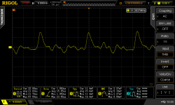
ES9018 output in voltage mode. It looks spiky, but the amplitude of HF clock leakage into the output is actually quite tiny. The spikes have ~ 1ns rise time and ~10mV amplitude. This is only 10V/µs ! Not worth panicking IMO.
As far as OP's TI DAC is concerned, probing with a scope would answer the question.
Attachments
I measured the resistance between two AVCC pins on ES9018. They're internally connected (proof: current drawn by one channel shows up on all the AVCC pins) but the resistance was surprisingly high, a few tenths of ohms. I agree that it's quite surprising and I expected much lower. I'm quoting from memory, unfortunately that ES9018 is soldered on a test board, so I can't measure it now.
A 25 um thick gold wire of 4 mm long is about 0.2 ohm. Above 10 MHz or so the inductive reactance dominates.
Last edited:
No sane manufacturer will wire bond high current pins with 25u gold wires. That’s what aluminum wire bonding is for. Check a power device of your choice. You will note multiple aluminum wires to the emitter/source pad(s).
I measured the resistance between two AVCC pins on ES9018. They're internally connected (proof: current drawn by one channel shows up on all the AVCC pins) but the resistance was surprisingly high, a few tenths of ohms.
Not sure what you mean by “current drawn by one channel shows up on all the AVCC pins”, perhaps you mean voltage? If what you measure is correct, this men’s all AVCC pads are not shorted by the metallization layers, but through diffusions. Meaning that it is absolutely required to connect all AVCC pins to the power supply.
- Home
- Source & Line
- Digital Line Level
- Low noise regulator for DAC & clock