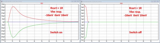
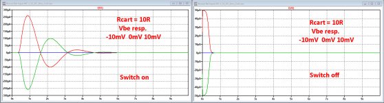
I get a 450mA pulse through the Cart at switch on when using a 1R Cart, resp. a 20mA pulse for a 10R Cart.
Pulse is very short, but wouldn't it be better when this could be eliminated?
T*I^2 (the melting current) is what really matters. This is here about 1E-9*(0.5)^2=250pA^2*sec. A ridiculous value, check out https://m.littelfuse.com/~/media/automotive/catalogs/littelfuse_fuseology.pdf page 5 and compare this value with a pulse shape of your choice.
Last edited:
Perhaps you could use a FET between the legs to shorten them until supply currents have settled, and then slowly open it so the servo can follow.
Or fasten up the servo during switch on.
The 1.5mA current through the 1 Ohm cart only happens when the delta Vbe between the two transistors is at a max of 10mV. For a selected pair of 2mV max delta Vbe, the currents are 500uV for 5-10 seconds. No MC cart is going to have problems dealing with that (or the 1.5mA worst case).
Its a different story of course if you run mA through the cart permanently which is what happens if you do not use a servo and you have a large Vbe differential between the transistors. I would not do that.
🙂
I think I found the solution I was looking for.
It's too late now.
Will show the results tomorrow.
Hans
It's too late now.
Will show the results tomorrow.
Hans
There is no reason to return R5 and R6 to 0V. Those could go to the -ve rail and then be capacitor filtered at say -10 or -12 V. This would help to define the collector currents more accurately and give the servo more room to correct the Vbe offsets. That said, if the +5 V rail will be supplied from something like a LM4562 you don’t want to be pulling more than 10 or 15 mA out in total.
I don’t think it is practical to use this circuit without selecting Q1 and Q2 for Vbe (2-3 mV) and ideally a reasonable hFE match.
Differences in emitter input resistance of the two transistors will translate into loss of CM rejection, but this should be small with good hFE match.
I don’t think it is practical to use this circuit without selecting Q1 and Q2 for Vbe (2-3 mV) and ideally a reasonable hFE match.
Differences in emitter input resistance of the two transistors will translate into loss of CM rejection, but this should be small with good hFE match.
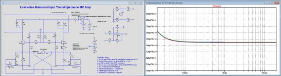
Here is what I made of it.
I always favour symmetrical designs, that's why I added a second servo.
A number of component were discarded, so in total component count hasn't increased.
I made a central base voltage reference, making the circuit independant of Hfe differences.
In this case Ic is 9.35mA, but can be easily adjusted.
Theoretical noise is sqrt ((2*Rbb + 2*1/2Gm + Rcart)/59.2)nV/rtHz
For Rbb=1.5R and Rcart=1R this calculates to 336nV/rtHz.
In the simulation I get 345nV/rtHz independent of Vbe differences, only 0.2dB off.
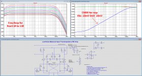
The images below are showing resp:
Freq Range and CMRR, Noise, and on-off response for resp. Rcart is 1R and 10R.
Not shown in what happens as a spike at switch on, that was previously in the hundreds of mA but now not exeeding 30uA for what it's worth.
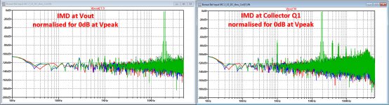
In the last image IMD is shown at the output for 19+20Khz at 2.5mV each, giving Vpeak = 5mV for Rcart = 1R.
Images are normalised to 5mV = 0dBr.
Quite obvious is that the 1Khz distortion product, visible in the collector of Q1 is no longer visible in Vout , because this 1Khz component has opposite polarity between Q1 and Q2 and cancel each other.
Visible is that the servos are perfectly doing their job, resulting in the same IMD for the used three Vbe differences of -10mV, 0mv and +10mV.
Hans
.
I always favour symmetrical designs, that's why I added a second servo.
A number of component were discarded, so in total component count hasn't increased.
I made a central base voltage reference, making the circuit independant of Hfe differences.
In this case Ic is 9.35mA, but can be easily adjusted.
Theoretical noise is sqrt ((2*Rbb + 2*1/2Gm + Rcart)/59.2)nV/rtHz
For Rbb=1.5R and Rcart=1R this calculates to 336nV/rtHz.
In the simulation I get 345nV/rtHz independent of Vbe differences, only 0.2dB off.
The images below are showing resp:
Freq Range and CMRR, Noise, and on-off response for resp. Rcart is 1R and 10R.
Not shown in what happens as a spike at switch on, that was previously in the hundreds of mA but now not exeeding 30uA for what it's worth.
In the last image IMD is shown at the output for 19+20Khz at 2.5mV each, giving Vpeak = 5mV for Rcart = 1R.
Images are normalised to 5mV = 0dBr.
Quite obvious is that the 1Khz distortion product, visible in the collector of Q1 is no longer visible in Vout , because this 1Khz component has opposite polarity between Q1 and Q2 and cancel each other.
Visible is that the servos are perfectly doing their job, resulting in the same IMD for the used three Vbe differences of -10mV, 0mv and +10mV.
Hans
.
Attachments
That looks very nice - I'll have to play with it. In a practical head amp, you can use a OPA2188/9 dual auto zero amp to do the Vbe nulling.
Do you think the CMRR is realistic? Any differences in gm will affect this surely, because re' will be different. The problem will be worse at low Rcart resistances. Is the balanced to single ended circuit presenting the same load on the collector loads?
Anyway, very nice angle on this 🙂
Do you think the CMRR is realistic? Any differences in gm will affect this surely, because re' will be different. The problem will be worse at low Rcart resistances. Is the balanced to single ended circuit presenting the same load on the collector loads?
Anyway, very nice angle on this 🙂
Last edited:
Cmrr of -90dB measured in the image for Rcart=1R, will be in real life a bit worse, somewhere between 60 and 80dB depending on the accuracy of the used resistors, just play with the model and also create two ZTX transistors with slightly different Hfe parameters to get a feeling for sensitivity.
And yes the load on both collectors is the same.
Because the servo’s will keep the emitter voltages the same, Gm for both transistors will be the same.
If not, it would have been evident in the IMD test where the slightest Gm difference will let the 1Khz component pop up, which is not the case.
Hans
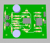
I’ll start laying a board out tomorrow and put the Gerbers up here.
For the +5 V supply you just divide the 18 V down and filter and buffer it with an LM4562 - same as X-Altra MC/MM
For the +5 V supply you just divide the 18 V down and filter and buffer it with an LM4562 - same as X-Altra MC/MM
Not shown in what happens as a spike at switch on, that was previously in the hundreds of mA but now not exeeding 30uA for what it's worth.
I suppose you are assuming the op amps powering up and servo-ing before the MC amp circuit fully powers up. That is, the op amp power supply is up before the MC amp supply. Possible, but not automatically true. Requires some sort of power sequencing circuit, to be 100% on the safe side.
I think anything less than a mA or two for a few seconds will be ok in a practical amp.
I note that on one of the ADI AZ opamps they recommended the opamp supplies are sequenced. I’ll go with the OPA2188/9 since I’m pretty familiar with those and don’t seem to have that issue.
I note that on one of the ADI AZ opamps they recommended the opamp supplies are sequenced. I’ll go with the OPA2188/9 since I’m pretty familiar with those and don’t seem to have that issue.
Last edited:
^Looks clean.
And the supply is Jan's Silent Switcher?
Btw, how quiet is its 5V output?
You don’t need ultra quiet +-18 V supplies because you leverage the opamp PSRR. Modern opamps are doing 120 dB at LF and the LM4562 is still an outstanding 70 or 80 dB at 100 kHz. A conventional well filtered 3 terminal type PSU is all that is needed.
I think anything less than a mA or two for a few seconds will be ok in a practical amp.
So do I, but that was not my point.
I’ll start laying a board out tomorrow and put the Gerbers up here.
For the +5 V supply you just divide the 18 V down and filter and buffer it with an LM4562 - same as X-Altra MC/MM
One half of the LM4562 for the output device, the other half for the buffer of the 5V supply.
I suppose you are assuming the op amps powering up and servo-ing before the MC amp circuit fully powers up. That is, the op amp power supply is up before the MC amp supply. Possible, but not automatically true. Requires some sort of power sequencing circuit, to be 100% on the safe side.
Nail on the head, and in reverse order at switch off.
This will need some clever additional circuitry that is also fail safe when mains supply drops out.
Just another challenge.
😀
Hans
One half of the LM4562 for the output device, the other half for the buffer of the 5V supply.
Yes - that’s what I’m planning.
Nail on the head, and in reverse order at switch off.
This will need some clever additional circuitry that is also fail safe when mains supply drops out.
Just another challenge.
😀
Hans
Easy enough to measure with a decent scope 😉
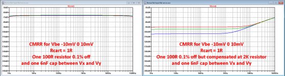
Further on the subject of CMRR and sensitivity on component matching.
Two 12nF caps are used to restrict the BW to 130Khz.
They would need a very high match to keep CMRR intact.
See first image below when using 1% caps.
When however replacing both caps by just one 6nF cap between Vx and Vy, FR stays the same without any matching at all and saving one cap.
When using 0.1% resistors, CMRR drops to -60dB, see second image.
This could be compensated to some degree with a small 20R pot in the 2K//390K resistor going to Gnd from the level shifting op-amp.
Hans
.
Attachments

Agree - the differential filter across Vx and Vy is a far better solution.
I think 60 dB is a good practical limit, but you can also always select (see Mark Johnson’s thread on this for example - a 0.05% match seems quite feasible in most cases from a 1% tolerance batch.
I am proposing to use 1206 SMD on the board.
I think 60 dB is a good practical limit, but you can also always select (see Mark Johnson’s thread on this for example - a 0.05% match seems quite feasible in most cases from a 1% tolerance batch.
I am proposing to use 1206 SMD on the board.
- Home
- Source & Line
- Analogue Source
- Low noise Balanced MC Pre