The SG505 is an outstanding very low distortion state variable oscillator SVF developed by Bruce Hofer while he was at Tektronix before being a co-founder of AP. His use of the SVF inspired most of the circuitry in the THD analyzer I designed (Audio article available on my website). As described below in another post, JFET Q1620 amplifies and inverts and amplifies the error signal at the positive input to U1520. This enhances the net error signal applied to the op amp and further reduces the already low distortion of the 5534. The feedforward/feedback arrangement of R1521, R1423, pot R1510 and R1525 comprises what is often called a Baxandall volume control, in which the positive input of the op amp is usually grounded. The distortion-reduction circuit of Q1620 is just for further reducing distortion of the output buffer stage, and is not necessary if the already-low distortion of the 5534 is acceptable (good enough for more than 90% of applications). If not the right JFET is chosen, this circuit may not function correctly and actually increase distortion. You can disable this circuit and still get excellent distortion results. You can disable it by just removing the JFET from the circuit. See if doing this makes the circuit work properly. If you do so, you should probably short R1524 to keep the positive input of the op amp at a low impedance to ground, as normally done in the Baxandall volume control. Note that in general use, the Baxandall volume control provides a good approximation to a logarithmic gain vs. pot rotation using a simple linear pot over a very wide range of gain, making it excellent for use as an audio volume control.I need some help with a particular circuit used in the Tektronix SG505.
I'm currently working on a DIY rebuild of the SG505, as a fun project and learning experience.
The generator itself is working according to the specifications as far as I can tell, but the output amplifier is adding significant harmonic distortion. The amplifier uses a JET and the function of it is a mystery for me.
Can somebody out here explain that to me please?
The JFET is a Tek p/n 151-1025-00, originally an SPF3036. The recommended replacement is the 2N4416, and that can be replaced by a J111. I have tried several different JFET's in the circuit, but without significant changes. Even when I take the JFET out of it's socket, there is little change in the FFT.
Here is my blog with the project details: Blog
Here is the SG505 manual: SG505 manual
The output amplifier section is on page 63.
Below is a small section of the circuit diagram.
Many thanks in advance!
Paul
Cheers,
Bob

Thank you Bob and Alex for the insights.
Now that we understand the purpose of the JFET, the next step is to find a replacement for the 151-1025-00 that is used. Unfortunately, I cannot find any details about it, nor for the original source, the SPF3036. It would greatly help if somebody would be kind/brave enough to measure the Gate voltage and the Drain voltage in the circuit or better yet, lift that JFET from any Tek instrument and put it on a Curve Tracer, or as a minimum, measure the Pinch off voltage and the rDS(on) for starters.
My goal is to see how far I can get the original SG505 working without making any changes at this moment, so I'm still trying to get the original output amplifier to work as close to the specifications as possible, before I start to use possible improvements, or use Bob's output amplifier section. 😉
So to continue with that quest, if I may in this thread, here is what my mouse-pal Bud (an ex-LT chip designer) found out while using LTspice for that particular circuit.
Many thanks for the collective insights, it proves the value of this forum.
Paul
Now that we understand the purpose of the JFET, the next step is to find a replacement for the 151-1025-00 that is used. Unfortunately, I cannot find any details about it, nor for the original source, the SPF3036. It would greatly help if somebody would be kind/brave enough to measure the Gate voltage and the Drain voltage in the circuit or better yet, lift that JFET from any Tek instrument and put it on a Curve Tracer, or as a minimum, measure the Pinch off voltage and the rDS(on) for starters.
My goal is to see how far I can get the original SG505 working without making any changes at this moment, so I'm still trying to get the original output amplifier to work as close to the specifications as possible, before I start to use possible improvements, or use Bob's output amplifier section. 😉
So to continue with that quest, if I may in this thread, here is what my mouse-pal Bud (an ex-LT chip designer) found out while using LTspice for that particular circuit.
Now that we’ve established that you need some gain, and the amount of gain has a direct effect on the distortion reduction, you have some options regarding the JFET.
The 2N4416 generates a typical gain of 5, which is not a lot, with the component values given by the output amp schematic. The 2N44116 datasheet shows IDSS varies from 5-15mA at room temperature. The transconductance, gfs, varies from 4.5-7.5 mmho over production. You are constrained by the high IDSS causing the JFET to enter triode mode, and therefore destroy the gain. And you are constrained by the lower value of transconductance, which reduces the gain from 5 to 4. IMHO it is bad design practice to base your design on the characteristics of a single device.
So what are you looking for in an acceptable JFET substitute? First of all it must not bias in the triode region. Therefore max IDSS must not exceed the supply voltage minus the JFET threshold voltage divided by the load resistors (about 17mA). Also, you’re looking for a typical transconductance larger than 6mmho (mS?) if you want to beat the 2N4416.
Alternatively, you could change the value of the load resistors, but making them smaller will increase supply current and power dissipation. You’re already at 75mW.
We are in agreement as to the operation of the JFET, but wrong in the suggestion that the J112 is a replacement. There is no typ or max IDSS spec for the J111/J112 in the datasheets that I've seen. If IDSS>17mA, then the VDS voltage will be less than 2V (for every J112), and put the JFET in triode mode with little gain. No gain = no THD improvement. So, instead of IDSS min, you should be looking for IDSS max <20mA.
I simulated the J112 (it is available in LTspice.) The VDS voltage is 1.3V and there is less than a 2X improvement in THD. The THD improvement when using the 2N4416 is a factor of 3.6.
I went to Digikey looking for acceptable candidates. I found the LSK170B (for about $7/each.) It has a very large gain (which requires additional compensation in my LTSpice simulation circuit) and yields a 15X improvement in THD. The 2SK1069-5 has an IDSS range of 5-12mA, with a forward admittance around 11mS, which would be nearly 2X better than the 2N4416, but I can't simulate it. The 2SK1069-5 is cheaper -- only 1.41/each, but you must buy 300 minimum (so...not cheaper).
I can probably find a few more, but the $7 LSK170B is probably your best bet right now if you don't want to change many component values. I'll keep looking.
Many thanks for the collective insights, it proves the value of this forum.
Paul
Hi Paul,
I may have missed something, but what happened to the original Tek JFET? Is it still alive? If so, check its IDSS value.
While it was in the circuit, did you check its operating point, such as its in-circuit drain voltage and thus voltage drop across its load resistor? There may also be a chance that the original part was a selected JFET. IDSS and pinchoff voltage can span a large range for JFETs. In a circuit like this, IDSS is probably more important than pinchoff voltage.
Don't rule out that there is something wrong other than the JFET.
Finally, to make sure there is not a problem of some other kind in the output buffer circuit, I would still disable the circuit by operating with no JFET and see if performance is good.
Make sure that the electrolytic coupling capacitor is the drain circuit is not defective in some way.
Cheers,
Bob
Hi Bob,
I do have two of the 151-1021-00 that is used in the SG505 AGC and found a few good alternatives.
The problem is that I do not have Q1620 p/n 151-1025-00 (the Motorola SPF3036) used in the output amp. Tek would have used another p/n if it was a selected version, so I'm very confident that it's "normal" part and it is also used in many other Tektronix instruments.
I tried several JFET's but they don't seem to improve the harmonic distortion, and the amp by itself produces significantly more distortion than the generator itself, that I found to be within the specifications. As I mentioned earlier, there's something fishy about my output amp contraption. Before I can zoom further in, I need to see if I can find a suitable alternative for the JFET, and Bud seemed to have found one, the LSK170C. Unfortunately, that part is not available to me in Europe, and going through Mouser or Digikey will set me back at least $30 for S&H alone.
That's why I'm searching for a good and available equivalent.
In the mean-time, I found a user that has an SG505 and was kind and brave enough to make some measurements in his unit.
He was not willing (I fully understand and appreciate that) to unsolder the part and measure the rDS(on) and Pinch-Off voltage.
Do we have enough data now to find other JFET's than the one Bud found?
Having said all that, before I can really zoom into the effects of the JFET, I need to improve my Twin-T notch filter setup (Dick Moore design) and significantly reduce the hum & noise. That's a side project that I'm working on right now.
I will put more information about that and the DIY build of the SG505 on my own Blog to not pollute this thread too much.
My understanding is that there could be some general merit in finding a good alternative for the 151-1025-00 that is used in many Tektronix instruments so that's the "excuse" for elaborating here. If you guys rather see a dedicated post, I'll start that.
Many thanks for the interest, I'm kinda overwhelmed by the quality responses!
I do have two of the 151-1021-00 that is used in the SG505 AGC and found a few good alternatives.
The problem is that I do not have Q1620 p/n 151-1025-00 (the Motorola SPF3036) used in the output amp. Tek would have used another p/n if it was a selected version, so I'm very confident that it's "normal" part and it is also used in many other Tektronix instruments.
I tried several JFET's but they don't seem to improve the harmonic distortion, and the amp by itself produces significantly more distortion than the generator itself, that I found to be within the specifications. As I mentioned earlier, there's something fishy about my output amp contraption. Before I can zoom further in, I need to see if I can find a suitable alternative for the JFET, and Bud seemed to have found one, the LSK170C. Unfortunately, that part is not available to me in Europe, and going through Mouser or Digikey will set me back at least $30 for S&H alone.
That's why I'm searching for a good and available equivalent.
In the mean-time, I found a user that has an SG505 and was kind and brave enough to make some measurements in his unit.
G - 0 V
S - 0 V
D - +12 V
V+ - 15,9 V
VR1620 = 3.9 V
R1620 = 510R
Idss = 7.65 mA
He was not willing (I fully understand and appreciate that) to unsolder the part and measure the rDS(on) and Pinch-Off voltage.
Do we have enough data now to find other JFET's than the one Bud found?
Having said all that, before I can really zoom into the effects of the JFET, I need to improve my Twin-T notch filter setup (Dick Moore design) and significantly reduce the hum & noise. That's a side project that I'm working on right now.
I will put more information about that and the DIY build of the SG505 on my own Blog to not pollute this thread too much.
My understanding is that there could be some general merit in finding a good alternative for the 151-1025-00 that is used in many Tektronix instruments so that's the "excuse" for elaborating here. If you guys rather see a dedicated post, I'll start that.
Many thanks for the interest, I'm kinda overwhelmed by the quality responses!
Q1620 is not rocket science. Given that R1620 is 510, the centered Vd is half the supply, 15/2=7.5 and Q1620 Vgs=0, the JFET is operating at Idss, so that the Idss should ideally be 7.7/510 ~=14.7mA. But if it's as little as 5mA or as much as 25mA, that's fine too, because the signal at the op-amp inputs is a "zero point", ie damn small. As long as Idss is not more than 25mA+ then you should be fine. So avoid J111, but J112 and J113 should be "OK". Note that 2N4416 Idss max is 15mA= perfect. You may want to find another JFET with Idss max = 15mA, or just hand select one. All it takes is a meter and bench power supply.
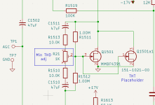
In an earlier Post, Bob Cordell mentioned that he added a 1K trimmer to tweak the Gate voltage of the JFET in the AGC section of his THD analyzer generator. I tried that with my DIY build of the SG505 and was amazed by the improvement. My 2nd H went from 0.00016% down to 0.000069% dropping the THD from 0.00021% to 0.00015%. Well done Bob, and thank you for the tip.
The circuit detail of the modification to adjust the 2ndH is attached.
This can also be done to existing SG505's.
I now also swapped out the original Tektronix 151-1021-00 JFET, and replaced it with an MMBF4391.
After re-tuning for the lowest 2ndH, I still have the same THD as above, but the 2ndH is even a bit lower at 0.000062%, so this is a good alternative.
In case you're interested and want to follow my activities, have a look here: Blog Post
The next step is to replace the NE5534's with the OPA1655DR.
Attachments
I tried this mod on my original SG505. The 2nd H went down from 0.000081% to 0.000077%. THD went down from 0.00019% to 0.00017%. Not a big improvement in my case.In an earlier Post, Bob Cordell mentioned that he added a 1K trimmer to tweak the Gate voltage of the JFET in the AGC section of his THD analyzer generator. I tried that with my DIY build of the SG505 and was amazed by the improvement. My 2nd H went from 0.00016% down to 0.000069% dropping the THD from 0.00021% to 0.00015%. Well done Bob, and thank you for the tip.
I have to add that 3rd H is dominant by being about 6 dB higher than 2nd H.
- Home
- Design & Build
- Equipment & Tools
- Low-distortion Audio-range Oscillator