opa1642 ... I did try that and got a worse result than OPA1612, OPA2156, OPA1656, and so on.
I had similar results. Also 1652 does not win. 1656/2156 - are the best!
Bootstrapping opamp's supply pin can mitigate common mode distortion, although bootstrapping from output may cause instability.
Bootstrapping from the input doesn't have a loop stability issue, and it has another benefit. Bootstrapping supply pin can also bypass the signal to the compensation capacitor, so the input stage is required little current to charge the cap which reduces the distortion of the input stage.
Bootstrapping from the input doesn't have a loop stability issue, and it has another benefit. Bootstrapping supply pin can also bypass the signal to the compensation capacitor, so the input stage is required little current to charge the cap which reduces the distortion of the input stage.
Attachments
What is the source of that bootstrapped op amp schematic?Bootstrapping opamp's supply pin can mitigate common mode distortion, although bootstrapping from output may cause instability.
Bootstrapping from the input doesn't have a loop stability issue, and it has another benefit. Bootstrapping supply pin can also bypass the signal to the compensation capacitor, so the input stage is required little current to charge the cap which reduces the distortion of the input stage.
Looks similar to Funasaka: https://www.proaudiodesignforum.com...S_v30n5_Feedforward_Floating_Power_Supply.pdf

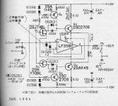
It's from a Japanese audio magazine. Toru Kuroda "Construct a super high performance MC only stereo preamp" Radio Gijutsu 1984 Jan. The article mentions the paper you post and the author's earlier article in '78.
Thanks for sharing.It's from a Japanese audio magazine. Toru Kuroda "Construct a super high performance MC only stereo preamp" Radio Gijutsu 1984 Jan. The article mentions the paper you post and the author's earlier article in '78.
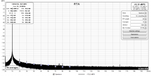
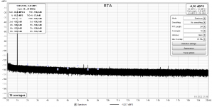
Here are my results with Victor's 1kHz oscillator + Twin-T notch 1kHz + LNA (OPA1656 with SE to Balance conversion) + Focusrite Forte as ADC.
One pic is with notch compensation and second one without (Twin-T has -50 dB attenuation on 1kHz, -8 dB on 2kHz, -4 dB on 3kHz).
Therefore 2nd harm. is -125-50+8= -167 dB, 3rd harm. is -126-50+4= -172 dB (but they are hidden in noise...).
THD is around -167 dB (0,000 000 45%)!
Martin
One pic is with notch compensation and second one without (Twin-T has -50 dB attenuation on 1kHz, -8 dB on 2kHz, -4 dB on 3kHz).
Therefore 2nd harm. is -125-50+8= -167 dB, 3rd harm. is -126-50+4= -172 dB (but they are hidden in noise...).
THD is around -167 dB (0,000 000 45%)!
Martin
Attachments
Last edited:
Yep, it works with analog RC gen as well but wiping up a DAC's output is more useful. I like to use the level control by software.
More like -157dB. You have to subtract the -10dB FS.Here are my results with Victor's 1kHz oscillator + Twin-T notch 1kHz + LNA (OPA1656 with SE to Balance conversion) + Focusrite Forte as ADC.
One pic is with notch compensation and second one without (Twin-T has -50 dB attenuation on 1kHz, -8 dB on 2kHz, -4 dB on 3kHz).
THD is around -167 dB (0,000 000 45%)!
Martin
Pls tell me why, harmonics are relative to the signal in REW not to the FS.More like -157dB. You have to subtract the -10dB FS.
See my first pic with notch compensation.
Martin
Right. -171.2-(-10.13)=-161dBPls tell me why, harmonics are relative to the signal in REW not to the FS.
See my first pic with notch compensation.
Martin
The gain of the LNA is +30 dB (not calibrated yet). Further I use gain of the Focusrite Forte line input (+20 dB) after the LNA.What's the gain of the post-filter LNA?
M.
Last edited:
I will check it later, but -161 dB seems more real than my previous measurement of -167 dB...Right. -171.2-(-10.13)=-161dB
Maybe I missed it but -161 dB relative to what?
What is the actual output level and load impedance?
What is the actual output level and load impedance?
0 dB is 2.7 Vrms output of the oscillator to the Twin-T notch - its load impedance is unknown to me (not measured yet, but I expect less than 10 kOhm - simulated is around 8 kOhm).Maybe I missed it but -161 dB relative to what?
What is the actual output level and load impedance?
So -161 dB (or less) is THD of the Victor's oscillator measured by the instrumentation explained above.
My example is about possibilities of the DIY for the low THD measurement in "home environment" without expensive gear.
Martin
Last edited:
Something isn't adding up...
You show a notch output level, post-LNA on the first FFT at -10 dBFS. There is about 50 dB post-notch gain which would put the actual 1 kHz notch level, pre-LNA at about -60 dBFS. You also mention that the notch depth is about 50 dB. That would put the oscillator output level, and the input to the notch at -10 dBFS.
If the above is true then the reference carrier level, 0 dBc, has to be close -10 dBFS.
The level of H2 is about -168 dBFS but only -158 dBFS below the 0 dBc, (-10 dBFS) carrier.
Subtracting the stated 8 dB insertion loss at H2 yields about -150 dBc.
Slightly OT:
I read earlier about the poor performance of the OPA1642. FWIW I just recently measured the output short-circuit current of several popular duals and the OPA1642 was the lightweight of the bunch at 28 mA. The OPA2604 and MC33078 were also lame at 30 mA. The OPA1612, LME49720 and multi-vendor 5532s measured in the 36-48 mA range. The King Daddy was the NJM4560 at 60 mA, the NJM2114 a close second at 56 mA and the NJM2068 coming in third at 52 mA. I can see how the 100 mA output of the OPA1656 would be beneficial.
My 0 dBc is 2.7 Vrms 1 kHz from oscillator.Something isn't adding up...
You show a notch output level, post-LNA on the first FFT at -10 dBFS. There is about 50 dB post-notch gain which would put the actual 1 kHz notch level, pre-LNA at about -60 dBFS. You also mention that the notch depth is about 50 dB. That would put the oscillator output level, and the input to the notch at -10 dBFS.
If the above is true then the reference carrier level, 0 dBc, has to be close -10 dBFS.
The level of H2 is about -168 dBFS but only -158 dBFS below the 0 dBc, (-10 dBFS) carrier.
Subtracting the stated 8 dB insertion loss at H2 yields about -150 dBc.
Slightly OT:
I read earlier about the poor performance of the OPA1642. FWIW I just recently measured the output short-circuit current of several popular duals and the OPA1642 was the lightweight of the bunch at 28 mA. The OPA2604 and MC33078 were also lame at 30 mA. The OPA1612, LME49720 and multi-vendor 5532s measured in the 36-48 mA range. The King Daddy was the NJM4560 at 60 mA, the NJM2114 a close second at 56 mA and the NJM2068 coming in third at 52 mA. I can see how the 100 mA output of the OPA1656 would be beneficial.
Notch is - 50 dB at 1 kHz.
LNA gain is around 30 dB (28.9 actually).
Forte input has gain 20 dB before ADC.
So we are back at about 2.7 Vrms which is around -10 dBFS of the ADC what you see on both pics. FS of the ADC is 7.75 Vrms (20 dBu).
All harmonics in REW charts are relative to the 2.7 Vrms (to our 0 dBc).
First pic is with SW compensation of the notch frequency response (imported cal file in REW). Here we see THD with all harmonics directly (with few dB of computation error).
Second one is not compensated, so we have to calculate real harmonics manually. H2 is 42 (50-8) dB down, H3 is 46 (50-4) dB down than we see on the pic relative to the dBc. Then H2 is -125-42=-167 dB, H3 is -126-46=-172 dB.
Hope, now it is more clear.
Martin
Last edited:
In my opinion, the easiest way to get true is to apply the same 2.7V RMS level (or any other known level) of 2 kHz or 3 kHz signal to the measurement input, and then calibrate 0 dB.
When I have time for it I will try it.In my opinion, the easiest way to get true is to apply the same 2.7V RMS level (or any other known level) of 2 kHz or 3 kHz signal to the measurement input, and then calibrate 0 dB.
Thank you.
Martin
0 dBFS is +20 dBu only at the minimum -12 dB gain.
You're applying 20 dB input gain in the Forte.
It be seen from the table below that the converter internal 0 dBFS is the typical 2V RMS or +8 dBu. (Clue is with the gain at -12 the Forte has a +20 dBu OL point.)
Is that value +20 more than the -12 minimum or +20 dB above unity?
From the Forte manual:

I think your results are hugely off because you're making assumptions about what 0 dBFS actually is with the gain you're applying.
Meter the A/D input with an actual AC voltmeter and use that for calibration.
I typically use 1V RMS at the A/D input and set the input gain pot so that I get -6 dBFS. That's true unity gain from the input connector to the A/D modulator and its measured below saturation and not near full scale. Then use 2V RMS as your 0 dBFS calibration value.
You're applying 20 dB input gain in the Forte.
It be seen from the table below that the converter internal 0 dBFS is the typical 2V RMS or +8 dBu. (Clue is with the gain at -12 the Forte has a +20 dBu OL point.)
Is that value +20 more than the -12 minimum or +20 dB above unity?
From the Forte manual:
I think your results are hugely off because you're making assumptions about what 0 dBFS actually is with the gain you're applying.
Meter the A/D input with an actual AC voltmeter and use that for calibration.
I typically use 1V RMS at the A/D input and set the input gain pot so that I get -6 dBFS. That's true unity gain from the input connector to the A/D modulator and its measured below saturation and not near full scale. Then use 2V RMS as your 0 dBFS calibration value.
Last edited:
- Home
- Design & Build
- Equipment & Tools
- Low-distortion Audio-range Oscillator