AndrewT said:Hi,
Finally add up the heatsinks. Is this smaller or larger than a dual or single chipamp feeding that load.
That all depends.
If you put devices in parallel on separate heatsinks, the sinks will be half as big.
If instead, as I have drawn, you put them together, then you will have the same size heatsink.
STILL, you will have lower die temperature. The point is not the size of heatsinks, it is sustained reliability.
That is what you get for "complexity."
If my recollection serves me, the point about "complexity" had already been made a number of times; the only factor not yet introduced or under consideration was the fact that a parallel config. does actually come with an advantage.
To be sure, one might think it less important than other potential advantages, or object to devices in parallel for aesthetic reasons. Still the advantage is real, and while there are responses to my post, there is nothing about the content of it.
Re: Re: Re: Multiple 1875
..provided you don't have to fit three of them into that space.
A single LM3875 or LM3886 provides the same amount of power. Look at the coincidence: 3 LM1875 with 3 K/W vs. 1 LM3875/LM3886 with 1 K/W results in exactly the same junction temperature. The LM3875/LM3886 will sound better and won't take up more space than three LM1875.
toolsresearch said:For that reason, again, obviously, it could be shoehorned into smaller spaces.
..provided you don't have to fit three of them into that space.
A single LM3875 or LM3886 provides the same amount of power. Look at the coincidence: 3 LM1875 with 3 K/W vs. 1 LM3875/LM3886 with 1 K/W results in exactly the same junction temperature. The LM3875/LM3886 will sound better and won't take up more space than three LM1875.
Re: Re: Re: Re: Multiple 1875
Actually, very much to the advantage of a single chip solution, the ratio of output watts to Pd is better for 3886 v. 3875, and 3875 is better than 1875. For example, with +/- 25 volts and 4 ohms, both 3875 and 3886 entail 32.4 and 32.9 Watts Pd respectively, comparable figures, and yet the 1% THD power out are 47 and 57 watts! With 1875 you are going to get the same 30 odd Watts of heat with only 20 Watts of power.
The efficiency advantage decreases with 8 ohm loads from better than 2 to 1 to something like 3 to 2.
That being said, the Theta jc advantage is not quite as described:
On p. 7 of the 1875 datasheet, it is 2 C/W and not 3. This is the same as the isolated packages, as you pointed out in another thread, and half as good as the unisolated packages.
Where the efficiency advantage is 3 to 2, and the theta jc advantage nothing, say, with a plastic ensconced 3875, then the three 1875 config. would enjoy a lower die temp.
pacificblue said:
A single LM3875 or LM3886 provides the same amount of power.
Actually, very much to the advantage of a single chip solution, the ratio of output watts to Pd is better for 3886 v. 3875, and 3875 is better than 1875. For example, with +/- 25 volts and 4 ohms, both 3875 and 3886 entail 32.4 and 32.9 Watts Pd respectively, comparable figures, and yet the 1% THD power out are 47 and 57 watts! With 1875 you are going to get the same 30 odd Watts of heat with only 20 Watts of power.
The efficiency advantage decreases with 8 ohm loads from better than 2 to 1 to something like 3 to 2.
That being said, the Theta jc advantage is not quite as described:
pacificblue said:
Look at the coincidence: 3 LM1875 with 3 K/W vs. 1 LM3875/LM3886 with 1 K/W results in exactly the same junction temperature.
On p. 7 of the 1875 datasheet, it is 2 C/W and not 3. This is the same as the isolated packages, as you pointed out in another thread, and half as good as the unisolated packages.
Where the efficiency advantage is 3 to 2, and the theta jc advantage nothing, say, with a plastic ensconced 3875, then the three 1875 config. would enjoy a lower die temp.
Re: Re: Re: Re: Re: Multiple 1875
Heat dissipation will be the same at the same output power. There is no efficiency advantage for the 3875/3886. Their advantage is that they can deliver more current, which leads to a higher achievable power.
On page 2 it is 3 K/W. If an isolated version of the 1875 existed, I bet it would also compare badly to the unisolated 1875.
Assuming it were so. What is the advantage? Certainly not sustained reliablility, because those ICs usually don't die of age. What terminates them are shorts at the output, working into too low loads and overheating. The LM3875/3886 come with on-board protection against all that. The LM1875 not. If you refit those protections externally, it will be even harder to justifiy the resulting increase in amplifier cost and size.
toolsresearch said:For example, with +/- 25 volts and 4 ohms, both 3875 and 3886 entail 32.4 and 32.9 Watts Pd respectively, comparable figures, and yet the 1% THD power out are 47 and 57 watts! With 1875 you are going to get the same 30 odd Watts of heat with only 20 Watts of power.
Heat dissipation will be the same at the same output power. There is no efficiency advantage for the 3875/3886. Their advantage is that they can deliver more current, which leads to a higher achievable power.
toolsresearch said:On p. 7 of the 1875 datasheet, it is 2 C/W and not 3. This is the same as the isolated packages, as you pointed out in another thread, and half as good as the unisolated packages.
On page 2 it is 3 K/W. If an isolated version of the 1875 existed, I bet it would also compare badly to the unisolated 1875.
toolsresearch said:then the three 1875 config. would enjoy a lower die temp.
Assuming it were so. What is the advantage? Certainly not sustained reliablility, because those ICs usually don't die of age. What terminates them are shorts at the output, working into too low loads and overheating. The LM3875/3886 come with on-board protection against all that. The LM1875 not. If you refit those protections externally, it will be even harder to justifiy the resulting increase in amplifier cost and size.
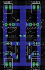
New Board
Hi
I am resurrecting this thread. I am about to make a LM1875 based amp and have prepared board for Amp & Power Supply. I will be trying to make my own boards (for the first time) with toner transfer and Ferric Cloride etching method. Attaching my drawings for Amp board and Power Supply
Any comments/ suggestions to improve the board or etching process is welcome.
PS: I am not an engineer by training so there may be more errors in the PCB
Thanks
Yatin
Attachments
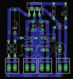
you have split your signal ground.
R2 goes to a different point from R1 (22k)
R5 goes to a different point from R1
C1 the DC blocking cap is on the wrong side of R2
There is no DC blocking cap on the NFB loop.
There is no RF attenuation on the input
You do not need 2 Power Grounds. One triplet twisted cable from PSU to AMP is good enough.
The speaker output is miss-wired.
I recommend that all your capacitor locations have at least two pin pitch options.
New Board
Thanks Andrew
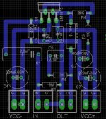
I have redone the board, I am using the typical application schematic in LM1875 datasheet with different values for capacitors and feedback. Only thing I added new is Inductor at output as I intend to use it as surround amp which will have long cable.
There is no DC blocking cap on the NFB loop
not understood can you please elaborate as to where this should be ?
There is no RF attenuation on the input
not understood can you please elaborate as to where and what this should be ?
You do not need 2 Power Grounds
Just made them so as to fix the connectors, are they harmful ? should I remove them ?
The speaker output is miss-wired
Hope I did them right this time around.
Thanks again for your valuable time
Regards
Yatin
Thanks Andrew
I have redone the board, I am using the typical application schematic in LM1875 datasheet with different values for capacitors and feedback. Only thing I added new is Inductor at output as I intend to use it as surround amp which will have long cable.
There is no DC blocking cap on the NFB loop
not understood can you please elaborate as to where this should be ?
There is no RF attenuation on the input
not understood can you please elaborate as to where and what this should be ?
You do not need 2 Power Grounds
Just made them so as to fix the connectors, are they harmful ? should I remove them ?
The speaker output is miss-wired
Hope I did them right this time around.
Thanks again for your valuable time
Regards
Yatin
Attachments
your first layout was better. V+ PG V- all in one 3way terminal block.
input signal hot and signal ground together and away from Power and speaker = good.
Just sort out the three signal grounds.
Put in the DC blocking capacitors that limit bandwidth and protect speakers.
Put in the missing RF filter.
Remove the output inductor.
input signal hot and signal ground together and away from Power and speaker = good.
Just sort out the three signal grounds.
Put in the DC blocking capacitors that limit bandwidth and protect speakers.
Put in the missing RF filter.
Remove the output inductor.
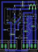
New Board
Thanks Andrew
I am attaching the latest board.
still not followed
"Put in the DC blocking capacitors that limit bandwidth and protect speakers.
Put in the missing RF filter."
Is there any schematic with the above 2 points which I can use ?
Thanks
Yatin
Thanks Andrew
I am attaching the latest board.
still not followed
"Put in the DC blocking capacitors that limit bandwidth and protect speakers.
Put in the missing RF filter."
Is there any schematic with the above 2 points which I can use ?
Thanks
Yatin
Attachments
you have fitted the two DC blocking capacitors (C1 & C2) to give you an AC coupled amplifier. This will protect the speaker from a faulty source.
National's datasheet shows an RF filter on the input.
It consists of just two components. A capacitor and a resistor. 1k0 & 680pF work for most builders, but you will find a wide range of values used by other builders. Your other post of the 3886 shows R11 & C9. What do these do?
The two 100nF decoupling caps are getting a bit far from the power pins.
I wonder if you could improve the layout (and save PCB area) if you bring the output down the right hand side?
Allow multi pin pitch for all your capacitors.
Widen the power rail and output traces and the pads.
Check your Zobel values. 1k0 (R5) & 220nF (C7?)
Last edited:
New Board
Thanks Andrew
I am trying to make another PCB with your suggestions incorporated.
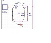
When you mean RF filter at Input, does it mean something like attached ?, I will be using 22K pot on the input for volume control, do you still fill RC filter of 1K0 & 680pF is necessary, if yes I will change the PCB accordingly.
Zobel values of 1K0 & 0.22uF are as per typical application in datasheet, do you suggest alternate values ?
Thanks for helping
Yatin
Thanks Andrew
I am trying to make another PCB with your suggestions incorporated.
When you mean RF filter at Input, does it mean something like attached ?, I will be using 22K pot on the input for volume control, do you still fill RC filter of 1K0 & 680pF is necessary, if yes I will change the PCB accordingly.
Zobel values of 1K0 & 0.22uF are as per typical application in datasheet, do you suggest alternate values ?
Thanks for helping
Yatin
Attachments
That's not 1k, that's 1R. Most people seem to recommend a value close to your speaker impedance, ie 8R.
post211.
the ratio of c1:c2 is wrong
Yes, you must bandlimit the amplifier (all amplifiers) at the input. Fit an RF filter.
Did you go and look at your 3886 post? what were those two components there for?
the ratio of c1:c2 is wrong
Yes, you must bandlimit the amplifier (all amplifiers) at the input. Fit an RF filter.
Did you go and look at your 3886 post? what were those two components there for?
New Board
Thanks Andrew
When you say RF filter at the input, what should be the corner freqency ? the config in the picture 680R x 470pF gives a freqency of 500,000Hz (1/2xPix680x470/10^-12)
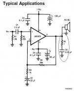
Frankly the 1K0 & 220pF are copied from the attached scematic, I have read somewhere that they act as RF filter to cut out hum and switching clicks from the other appliances which may be connected on the same electrical connection as the Amp.
Thanks again for your time, I am still on learning curve, not being an engineer makes it still steaper !!!!!
Regards
Yatin
Thanks Andrew
When you say RF filter at the input, what should be the corner freqency ? the config in the picture 680R x 470pF gives a freqency of 500,000Hz (1/2xPix680x470/10^-12)
Frankly the 1K0 & 220pF are copied from the attached scematic, I have read somewhere that they act as RF filter to cut out hum and switching clicks from the other appliances which may be connected on the same electrical connection as the Amp.
Thanks again for your time, I am still on learning curve, not being an engineer makes it still steaper !!!!!
Regards
Yatin
Attachments

we are getting there.
Now add the High pass filter at the input.
This will convert the amplifier to AC coupled.
I like the differentiation between GNDa and GND.
What about the speaker return?
I would expect pin5 to require decoupling.
National do not expressly say which or if both supplies need decoupling.
Now add the High pass filter at the input.
This will convert the amplifier to AC coupled.
I like the differentiation between GNDa and GND.
What about the speaker return?
I would expect pin5 to require decoupling.
National do not expressly say which or if both supplies need decoupling.

Sorry for DP, but cant find edit button.
Is this layout good for etching/or need to make some changes?
Is this layout good for etching/or need to make some changes?
Zobel
By the 1R resistor for speaker zobel, you've called for a series capacitor with high internal loss, which is a polyester dip cap. That is the intention of National Semiconductor as that is the typical cap for this role. The pin spacing for speaker zobel capacitor doesn't fit. The capacitor isn't that big.
Alternatively, you could go about 4 ohms for speaker zobel, which allows a wide varieity of caps for speaker zobel. However, the size of that 220nF cap will be the exact same size pin spacing as your 100nF caps.
The zobel is in place, but the other half of the thile-small speaker output filter seems to be missing (a small easy inductor and a 3w resistor, typically seen on discrete solid state amplifiers). Omission may slightly raise the idle operating temperature of the amplifier. You might want to check and see if there's an energy consumption difference (heatsink temp difference) at idle.
The 1k series to 22uF is a bass blocker and if you intend to allow low bass to have normal gain (and the midrange to have a normal proportion) then perhaps you would enjoy a larger size cap. Currently, the board's listed values will make the voice band louder than expected, which is very popular for television amplifiers.
A 100uF (and much larger) NFB cap is workable to expand the bandwidth to include bass at proportional gain, selection of capacitor size can be based on either your estimation of Either bass tonality preferences Or the "most expected" woofer size that will be used with the amplifier.
The input filter needs to block at least as much bass as the NFB cap, in order for clean results. Aim it about an octave lower than the "expected" speaker's roll-off.
A 100uF cap is technically a bit small; however, it is fortunately small enough to avoid high frequency failure mode. Another option is 330uF//330nF (with the added smaller cap restoring treble clarity to seemly proportion).
If you happen to want to drive that amplifier directly from a computer or mp3 player, you can change the 1k to 820R and you can change the 20k to 24k. That change to the gain setting (24k, 820R) would give a significant boost, helpful to popular modern source devices.
Hey all! In this rainy day I have made a PCB too! 🙂
Feel free to comment! Cheers!
By the 1R resistor for speaker zobel, you've called for a series capacitor with high internal loss, which is a polyester dip cap. That is the intention of National Semiconductor as that is the typical cap for this role. The pin spacing for speaker zobel capacitor doesn't fit. The capacitor isn't that big.
Alternatively, you could go about 4 ohms for speaker zobel, which allows a wide varieity of caps for speaker zobel. However, the size of that 220nF cap will be the exact same size pin spacing as your 100nF caps.
The zobel is in place, but the other half of the thile-small speaker output filter seems to be missing (a small easy inductor and a 3w resistor, typically seen on discrete solid state amplifiers). Omission may slightly raise the idle operating temperature of the amplifier. You might want to check and see if there's an energy consumption difference (heatsink temp difference) at idle.
The 1k series to 22uF is a bass blocker and if you intend to allow low bass to have normal gain (and the midrange to have a normal proportion) then perhaps you would enjoy a larger size cap. Currently, the board's listed values will make the voice band louder than expected, which is very popular for television amplifiers.
A 100uF (and much larger) NFB cap is workable to expand the bandwidth to include bass at proportional gain, selection of capacitor size can be based on either your estimation of Either bass tonality preferences Or the "most expected" woofer size that will be used with the amplifier.
The input filter needs to block at least as much bass as the NFB cap, in order for clean results. Aim it about an octave lower than the "expected" speaker's roll-off.
A 100uF cap is technically a bit small; however, it is fortunately small enough to avoid high frequency failure mode. Another option is 330uF//330nF (with the added smaller cap restoring treble clarity to seemly proportion).
If you happen to want to drive that amplifier directly from a computer or mp3 player, you can change the 1k to 820R and you can change the 20k to 24k. That change to the gain setting (24k, 820R) would give a significant boost, helpful to popular modern source devices.
Thank you very much! 🙂 I appreciate your help! 🙂
And another question - what values would be the best for 3w resistor and inductor?
And another question - what values would be the best for 3w resistor and inductor?
Last edited:
Thank you very much! 🙂 I appreciate your help! 🙂
And another question - what values would be the best for 3w resistor and inductor?
10. As in 10 ohms and 10 turns around a bic pen lid. 🙂
Ah, this was from memory. You might want to double check with examples already posted over at the Solid State forum.
- Status
- Not open for further replies.
- Home
- Amplifiers
- Chip Amps
- LM1875 PCB, Which To Use