Hi
i did a measurement at my ebay kit with bests parts and I look at the DC offset to go ahead with my double amp - paralleling 2 chips. i soldered a 0R1 5W resistor . i observed -2mV/-1,9mV with my lab power supply at +/-27V. with +/- 25V i get a little bit less -1,8mV/-1,7mV.
then i did a test to look again the gain setting of both amps. i forget to DMM at the output and start with a sweep of 10Hz to 35khz and see that the DC offset is going up/down. this forced me to look closer:
+/-27V power supply - amp 1
400mVrms input with 1khz - 29,2mV Dc offset - 9,04Vrms at 8R
500mVrms input with 1khz -15mV Dc offset - 11,1Vrms at 8R - 15Watt
500mVrms input with 8khz - 53,3mV Dc offset - 11,1Vrms at 8R
500mVrms input with 10khz- 42,7mV Dc offset - 11,1Vrms at 8R
...................................................
chris
I notice you have a gain of a bit more than 22. 2mV offset at the output with a gain of 22 is very good - with less gain the output offset should also be less.
DC-offset is normally measured without signal. I see you measure a DC-offset with a considerable signal level. Is that an offset you measure between the two LM1875 outputs using a DMM? If so,is your DMM put in DC or AC setting?
You are needed in politics.
I'm not into politics. Been there, done that, but it's not my cup of tea.
What-about-such-a-solution?
That should work just fine. The 15V rails must be tightly regulated, obviously.
If we use LM1875 from the same production batch, I expect that they will clip (saturate) at very similar levels.
It is not about the same production batch, but more about the gain mismatch and offset difference between the output stages that would lead to different clipping levels. If we match the gain resistors to within 1R and trim the offset at the outputs to within 1mV, there should be no problems. It's just that little "IF" that needs a lot of our attention 😉.
I notice you have a gain of a bit more than 22. 2mV offset at the output with a gain of 22 is very good - with less gain the output offset should also be less.
DC-offset is normally measured without signal. I see you measure a DC-offset with a considerable signal level. Is that an offset you measure between the two LM1875 outputs using a DMM? If so,is your DMM put in DC or AC setting?
Hi FF
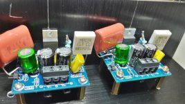
i wanted to go ahead with my normal mono kit (ebay kit) with the best parts to use 2 chips per side. see pic. i made the experience at this pcb that shorted the input signal or leave that input open but connected is a very similar. So i just power up one board and look without signal at the DC offset after the 0R1 resistor....e.g. -2mV. then i push an input signal into the amp and tried a sweep...then i saw the DC offset was going up/down.
as Preamp remind me i forgot to couple my frequency generator with a cap. so yes my freq. generator produce DC offset. my suggested 30mV was too much because with gain of 22/23 .
i had at the max point 62mV DC (650mV input 12khz)- i have to recheck my scope probe/measurement.
it looks like a higher gain (mono ebay kit) is more stable and not so critical as a composite amp with gain 2-4 LM1875.....but thats not our target here...😉
chris
Attachments
Gain in the LM1875 power stages.
The gain in the LM1875 power stages should be set to allow the controlling OP-AMP, in a composite amplifier configuration, to operate at signal levels with the lowest distortion levels.
Personally, I use OP-AMPs like LM4562 (LME49720), OPA2134 and NE5532 for audio purposes. I am aware that newer high performance OP-AMPs like OPA1612, OPA1622 and eventually OPA1688 are available as well. OPA1612 has slightly better specifications than LM4562 but is not supplied in the DIY friendly DIL-8 housing allowing an IC socket for easy replacement. A more pronounced quality of OPA1612 is the better performance at low supply voltages which is, however, of little importance for the present application.
A common characteristic of these OP-AMPs is that their distortion decreases steadily with increase in signal level until a point where the distortion rises very rapidly with further increase in amplitude. The trick is evidently to use the OP-AMPs at good signal amplitude levels but below where the distortion rises rapidly and such that there is a safe margin to that rise in distortion level.
The datasheet for LM1875 states that a gain of more than 10 times should be used for stability reasons. We often use LM1875 with gains around 20 times and could consider what would be the result of using an LM1875 with a gain of 20 times in a composite amplifier configuration.
An LM1875 with +/-25V supply can reach a maximum of about 20V on the output. 20Vp at the output and with a gain of 20 times means an input signal of 1Vp. That 1Vp will be the maximum amplitude of the controlling OP-AMP. With higher signal levels than 1Vp from the OP-AMP, the LM1875 output will reach saturation (clipping) and that serves no purpose. But, 1Vp is below where the OP-AMP has its optimum operational point as described in the following. Further, a gain of 20 times would leave more noise at the output of the LM1875. This is why it is very convenient that an LM1875 can be used at gain levels at least down to 2 times such that the LM1875 gain can be adapted to the optimum OP-AMP operational point.
The distortion curves versus signal amplitude depend on the OP-AMP supply voltage. Generally, an OP-AMP performs better the higher supply voltage it operates from. Some OP-AMPs can handle supply voltages up to +/-17-18V. Most OP-AMPs operate very well at +/-15V supply and all the types I mention above can be used at +/-15V. It is very convenient to use the general supply of the power amplifier also for the controlling OP-AMP but in the sense that between each general power supply rail and the OP-AMP power supply terminals, two linear regulators are inserted to keep the OP-AMP supply voltage at constant 15V disregarding voltage swings in the general supply voltage. As OP-AMPs use little current, a voltage drop down to 2V across each regulator is realistic even without use of low-drop regulators. With 2V drop, 15V out becomes 17V at the input of the voltage regulators. Then, the operational range for the general supply becomes +/-17V to +/-25V. That is a comfortably wide supply range.
I would like that the LM4562 can be used near its optimum operational point because I hardly find any OP-AMP with much lower distortion as long as the supply voltage is generous. LM4562 is easy to find, not expensive and can be supplied in the traditional DIL-8 package for DIY experiments. The LM4562 datasheet is elaborate on distortion curves (IMD) versus signal amplitude in figures 24-36. With +/-15V supply, figures 24, 28 and 32 apply.
For the LM4562, with +/-15V supply and 600 Ohm loading as shown in figure 28, distortion raises very rapidly above 5V. Though not explicitly stated, the 5V can be assumed to be RMS voltage as the curve relates to distortion and distortion relates to sine-wave signals, normally characterized by RMS amplitude. To leave a bit of amplitude margin from the steep raise in distortion, I propose to use the LM4562 until 4Vrms amplitude. 4Vrms corresponds to 5.7Vp. Thus, 5.7Vp at the input of an LM1875 power stage should leave the assumed clipping limit voltage of 20Vp at the LM1875 output. 20Vp/5.7Vp= 3.5. The gain of an LM1875 power stage should be 3.5 times to use LM4562 well.
For OPA1612, figure 11 of that datasheet shows the THD+N versus amplitude but without specifying the supply voltage. It is indicated that the OPA1612 output can go closer to the supply rails than for LM4562 before the distortion increases rapidly. Thus, with a gain suited for LM4562 also OPA1612 will work well. Would the LM1875 gain be reduced to suit the OPA1612 best, the LM4562 would operate with a high level of distortion near the maximum output of the LM1875.
OPA2134 seems to have a curve-shape similar to that of LM4562 such that the LM1875 gain, when adapted to LM4562, should also work well with OPA2134. Similar distortion/amplitude information is not provided for NE5532.
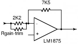
As I wish to keep the input impedance of each LM1875 power stage so high that one 600 Ohm driving OP-AMP can drive three LM1875 power stages in parallel, I suggest to use 2K2 as the value of the input resistor. For a gain of 3.5, the feedback resistor should be 7700 Ohm. The nearest standard value is 7K5.
The gain in the LM1875 power stages should be set to allow the controlling OP-AMP, in a composite amplifier configuration, to operate at signal levels with the lowest distortion levels.
Personally, I use OP-AMPs like LM4562 (LME49720), OPA2134 and NE5532 for audio purposes. I am aware that newer high performance OP-AMPs like OPA1612, OPA1622 and eventually OPA1688 are available as well. OPA1612 has slightly better specifications than LM4562 but is not supplied in the DIY friendly DIL-8 housing allowing an IC socket for easy replacement. A more pronounced quality of OPA1612 is the better performance at low supply voltages which is, however, of little importance for the present application.
A common characteristic of these OP-AMPs is that their distortion decreases steadily with increase in signal level until a point where the distortion rises very rapidly with further increase in amplitude. The trick is evidently to use the OP-AMPs at good signal amplitude levels but below where the distortion rises rapidly and such that there is a safe margin to that rise in distortion level.
The datasheet for LM1875 states that a gain of more than 10 times should be used for stability reasons. We often use LM1875 with gains around 20 times and could consider what would be the result of using an LM1875 with a gain of 20 times in a composite amplifier configuration.
An LM1875 with +/-25V supply can reach a maximum of about 20V on the output. 20Vp at the output and with a gain of 20 times means an input signal of 1Vp. That 1Vp will be the maximum amplitude of the controlling OP-AMP. With higher signal levels than 1Vp from the OP-AMP, the LM1875 output will reach saturation (clipping) and that serves no purpose. But, 1Vp is below where the OP-AMP has its optimum operational point as described in the following. Further, a gain of 20 times would leave more noise at the output of the LM1875. This is why it is very convenient that an LM1875 can be used at gain levels at least down to 2 times such that the LM1875 gain can be adapted to the optimum OP-AMP operational point.
The distortion curves versus signal amplitude depend on the OP-AMP supply voltage. Generally, an OP-AMP performs better the higher supply voltage it operates from. Some OP-AMPs can handle supply voltages up to +/-17-18V. Most OP-AMPs operate very well at +/-15V supply and all the types I mention above can be used at +/-15V. It is very convenient to use the general supply of the power amplifier also for the controlling OP-AMP but in the sense that between each general power supply rail and the OP-AMP power supply terminals, two linear regulators are inserted to keep the OP-AMP supply voltage at constant 15V disregarding voltage swings in the general supply voltage. As OP-AMPs use little current, a voltage drop down to 2V across each regulator is realistic even without use of low-drop regulators. With 2V drop, 15V out becomes 17V at the input of the voltage regulators. Then, the operational range for the general supply becomes +/-17V to +/-25V. That is a comfortably wide supply range.
I would like that the LM4562 can be used near its optimum operational point because I hardly find any OP-AMP with much lower distortion as long as the supply voltage is generous. LM4562 is easy to find, not expensive and can be supplied in the traditional DIL-8 package for DIY experiments. The LM4562 datasheet is elaborate on distortion curves (IMD) versus signal amplitude in figures 24-36. With +/-15V supply, figures 24, 28 and 32 apply.
For the LM4562, with +/-15V supply and 600 Ohm loading as shown in figure 28, distortion raises very rapidly above 5V. Though not explicitly stated, the 5V can be assumed to be RMS voltage as the curve relates to distortion and distortion relates to sine-wave signals, normally characterized by RMS amplitude. To leave a bit of amplitude margin from the steep raise in distortion, I propose to use the LM4562 until 4Vrms amplitude. 4Vrms corresponds to 5.7Vp. Thus, 5.7Vp at the input of an LM1875 power stage should leave the assumed clipping limit voltage of 20Vp at the LM1875 output. 20Vp/5.7Vp= 3.5. The gain of an LM1875 power stage should be 3.5 times to use LM4562 well.
For OPA1612, figure 11 of that datasheet shows the THD+N versus amplitude but without specifying the supply voltage. It is indicated that the OPA1612 output can go closer to the supply rails than for LM4562 before the distortion increases rapidly. Thus, with a gain suited for LM4562 also OPA1612 will work well. Would the LM1875 gain be reduced to suit the OPA1612 best, the LM4562 would operate with a high level of distortion near the maximum output of the LM1875.
OPA2134 seems to have a curve-shape similar to that of LM4562 such that the LM1875 gain, when adapted to LM4562, should also work well with OPA2134. Similar distortion/amplitude information is not provided for NE5532.
As I wish to keep the input impedance of each LM1875 power stage so high that one 600 Ohm driving OP-AMP can drive three LM1875 power stages in parallel, I suggest to use 2K2 as the value of the input resistor. For a gain of 3.5, the feedback resistor should be 7700 Ohm. The nearest standard value is 7K5.
Attachments
From your photos it looks like the amps are capacitor coupled already, so the DC offset can not be from your generator. Probably just the multimeter that can not cope such a huge superimposed AC while in DC mode?
Higher gain (like 30x compared to 3x) mostly helps with stability, yes, but usually has worse noise and distortion performance.
Higher gain (like 30x compared to 3x) mostly helps with stability, yes, but usually has worse noise and distortion performance.
Hi FF
i wanted to go ahead with my normal mono kit (ebay kit) with the best parts to use 2 chips per side. see pic. i made the experience at this pcb that shorted the input signal or leave that input open but connected is a very similar. So i just power up one board and look without signal at the DC offset after the 0R1 resistor....e.g. -2mV. then i push an input signal into the amp and tried a sweep...then i saw the DC offset was going up/down.
as Preamp remind me i forgot to couple my frequency generator with a cap. so yes my freq. generator produce DC offset. my suggested 30mV was too much because with gain of 22/23 .
i had at the max point 62mV DC (650mV input 12khz)- i have to recheck my scope probe/measurement.
it looks like a higher gain (mono ebay kit) is more stable and not so critical as a composite amp with gain 2-4 LM1875.....but thats not our target here...😉
chris
Hi Chris,
I will join Preamps conclusion that you cannot rely on measuring DC-offset correctly when you have a much bigger AC mixed with the small DC voltage. It is like listening if you can hear noise inside your living from a road 200m away when your stereo play at loud level. That the DDM display values change is an indication that the measurement is not precise.
To get away with such a measurement would require a very efficient low pass filter and then the DMM sampling rate would be very low.
Thanks FF for your advise...
i think its better to use the scope probe at the output and switch between DC/AC coupling....to look at the eventually DC offset during different frequencies.
at post 88 i did the simple paralleling and so far no problems. i want to finish my 2x1875 amp - so i want to keep that investigation short as possible to go to the composite amp.
chris
NB: I read that Finland is going to try a four day working week, which I find courageous and encouraging. But, I notice you are active at 5:36 in the morning. Is that a less known consequence? 😀
That is completely fake news... 🙂
I myself am self employed, so I work 25hours /day, 8days /week and 13months /year...
🙂
My proto PCBs are on the plane, so I can start testing the composite behaviour hopefully soon and report back...
The Finnish mail service is not, however, working 8days/ week so it may still take awhile before I receive them.
🙂
That's what made father Christmas decide to settle in Finland. The month of December is terribly busy so he needs that kind of working attitude.I myself am self employed, so I work 25hours /day, 8days /week and 13months /year...
Keep going............
Thanks FF for your advise...
i think its better to use the scope probe at the output and switch between DC/AC coupling....to look at the eventually DC offset during different frequencies.
at post 88 i did the simple paralleling and so far no problems. i want to finish my 2x1875 amp - so i want to keep that investigation short as possible to go to the composite amp.
chris
The scope-probe can remove the small DC but how are you going to remove the larger AC signal so you can see the small DC level?
That's what made father Christmas decide to settle in Finland. The month of December is terribly busy so he needs that kind of working attitude.
Keep going............
Father Xmas has solved the time problem. He has a machine which slows down the rotation speed of the planet. That way he has as much time as he needs to travel to every home in every country in the world.
Machine is shown in Rovaniemi Lapland, Arctic Circle, Santapark, if someone is seriously interested in it...
🙂
But back to topic now...
The scope-probe can remove the small DC but how are you going to remove the larger AC signal so you can see the small DC level?
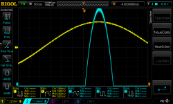
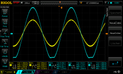
i used a input signal with 400mV rms in = its a bout 9Vrms out into 8R...and I switched the voltage base in a finer region and use the horizontal trimmer to look at the upper point. (you have to scroll a lot..) then i switched between DC and AC.
pic 1 DC the blue line is on the top of the scope Voltage/div is 134mV
pic 2 AC the blue line is not on the top so its about a half of the 134mV = 65mV
is that a correct methode😀
chris
Attachments
...amp dead ???
Hi
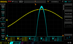
i found a maybe a dead chip. this chip i tested yesterday at post 170.
at the beginning everything looks fine but after 2 minutes the negative half is going to clipping. and keep this .....input is about 400mVrms so about 5Watt into 8R.
i changed nothing...chip dead?
chris
Hi
i found a maybe a dead chip. this chip i tested yesterday at post 170.
at the beginning everything looks fine but after 2 minutes the negative half is going to clipping. and keep this .....input is about 400mVrms so about 5Watt into 8R.
i changed nothing...chip dead?
chris
Attachments
Hi
i found a maybe a dead chip. this chip i tested yesterday at post 170.
at the beginning everything looks fine but after 2 minutes the negative half is going to clipping. and keep this .....input is about 400mVrms so about 5Watt into 8R.
i changed nothing...chip dead?
chris
The chip is obviously not "dead" as you still have an output. The chip may have a degraded performance. The curve you show, is that this LM1875 alone without any connection to the second LM1875 board?
Is there a possibility that you have a DC offset in your input signal?
I guess you have a capacitor in the line from the LM1875 inverting input to signal ground? Such a capacitor may be the reason for a small offset voltage I believe.
i used a input signal with 400mV rms in = its a bout 9Vrms out into 8R...and I switched the voltage base in a finer region and use the horizontal trimmer to look at the upper point. (you have to scroll a lot..) then i switched between DC and AC.
pic 1 DC the blue line is on the top of the scope Voltage/div is 134mV
pic 2 AC the blue line is not on the top so its about a half of the 134mV = 65mV
is that a correct methode😀
chris
Hi Chris,
Measuring voltage offset I find difficult as long as you (probably) have at least one capacitor in the signal path. Assuming that 65mV at the output is right, with a gain of 22 times that corresponds to 3mV at the input. The voltage at a capacitor in the signal line between the inverting input and signal ground may easily slide 3mV and cause what we interpret as LM1875 input offset.
The LM1875 you just mentioned that clips at negative voltage before positive voltage may also be the result of an asymmetrical operational point caused by this capacitor. To check that seemingly degraded LM1875, we have to take it out of a parallel circuit with the other LM1875 board, temporarily deactivate the capacitor by a short circuit and test the LM1875 with a sine-wave without DC-offset. Still asymmetrical clipping?
The chip is obviously not "dead" as you still have an output. The chip may have a degraded performance. The curve you show, is that this LM1875 alone without any connection to the second LM1875 board?
Is there a possibility that you have a DC offset in your input signal?
I guess you have a capacitor in the line from the LM1875 inverting input to signal ground? Such a capacitor may be the reason for a small offset voltage I believe.
Hi FF
the amp is "alone" not in paralleling with the second amp. the cap is exactly like the ebay (schoolies amp) board schematic. (nichicon ues 100µF)
chris
Hi Chris,
....
Hi Chris,
Measuring voltage offset I find difficult as long as you (probably) have at least one capacitor in the signal path. Assuming that 65mV at the output is right, with a gain of 22 times that corresponds to 3mV at the input. The voltage at a capacitor in the signal line between the inverting input and signal ground may easily slide 3mV and cause what we interpret as LM1875 input offset......?
no paralleling of amp 1+2. before i want to do that i tried this tests the amps separately to be sure everything is ok...
i have to avoid with better/correct implementation at my generator to avoid the Dc offset ! - i have to recheck this...maybe bad contact...
chris
Hi FF
the amp is "alone" not in paralleling with the second amp. the cap is exactly like the ebay (schoolies amp) board schematic. (nichicon ues 100µF)
chris
Hi Chris,
To check this LM1875 we need to put it in the simplest configuration. Short-circuit temporarily the 100uF Nichicon. Apply a sine-wave signal (1KHz) without a DC component between the non-inverting input and signal ground. Increase slowly the input signal amplitude until clipping at the output. Is the clipping still clearly asymmetrical?
NB: Make sure that the non-inverting input is not only connected through a capacitor. All amplifier inputs must have a DC signal path. This is why you often have a resistor between the non-inverting input and signal ground.
Last edited:
Miscellaneous.
In order to compensate for common-mode bias currents at the two input terminals (inverting and non-inverting) of amplifier chips, I have learned to use impedance balancing. Bias currents at the two inputs will, with resistance at the inputs, transform into offset voltage at the inputs. The trick with common-mode input currents is to have the same resistance seen from each of the two input pins such that the change in offset voltage is the same for both inputs and turn into a less problematic common-mode voltage.
With 2K2 as input resistor and 7K5 as feedback resistor, the inverting input sees a resulting resistance of 1K7. 1K8 is the closest standard value and will be used at the non-inverting input.
For the Zobel network used at the output of an LM1875, 1R and 220nF in series are recommended. During my test of a single LM1875 in low gain configuration, I experimented a little with the Zobel network as well. 1 Ohm for damping seemed the best but the 220nF could be reduced to 100nF without negative effects. I propose to keep the initial values of 1R and 220nF as they seem quite appropriate in practical test.
For power line decoupling, the LM1875 datasheet recommends a 100uF capacitor in parallel with a 100nF capacitor for each rail. The 100nF probably serves to prevent HF-oscillation in the LM1875 chip. The 100uF prevents LF-oscillation and provides general energy storage. 100uF does not allow for much energy to be stored and the total capacitance on each supply rail should be considerably higher to ensure good bass performance. In order to prevent the LM1875 from oscillation, a part of the total supply rail decoupling needs to be physically close to the supply terminals of each LM1875. This means that two electrolytic capacitors with moderate diameter have to be placed near the 100nF capacitors and as close to the LM1875 supply terminals as possible, for each LM1875. Such two capacitors, I would choose in the range 220uF-1000uF and with a voltage rating of 35V minimum.
Depending on the output power of the amplifier and the power source used, a total of 4700uF-20000uF is needed on each supply rail. Most can be located at a further distance from the LM1875 chips.
During my test of a single LM1875 in low gain configuration, I experimented a little with an eventual capacitor across the feedback resistor. With a square-wave signal as input and at the output, a small 100pF capacitor would make the square-wave at the output look more perfect without tendency of overshoot. I suggest adding such 100pF across the feedback resistor. At least I will try when a more permanent version of the parallel power stage has been build.
A Thiele compensation network serves to compensate for capacitance at the amplifier output, often caused by the speaker cables. For the component values I had to seek guidance in datasheets. In the LM1875 datasheet I found no hint to such a Thiele compensation. Anyway, it would have to be a Thiele network for two or three LM1875 in parallel, not just for a single LM1875. For the LM3886 chip I found some guidance advising 0.7uH in parallel with 10R/(5W). If these are optimum values for our use I cannot tell and any knowledge on the matter is highly appreciated. Do tests with capacitance at the output need to be carried out to determine the values? One Thiele compensation network will be used on the common output of all parallel LM1875 power stages.
Attachments

- Home
- Amplifiers
- Chip Amps
- LM1875 in parallel configuration and used in a composite amplifier.