jkeny said:No I don't think posting the board would be just - Steve has given us this schema & he has boards (which was not the reason he started the thread) so I think in all fairness his IP should be protected - give the man something back for his generosity shown here!
Good on Ya, OS - three variants - should be interesting
No Heatsinking on DX board - I wonder is this the root of his big offset problem on his old board?
Edit: cross posts with Thomas
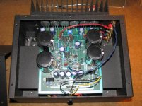
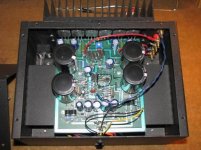
When Carlos and his constructing friend mount the finals to the heat sink assembly it should look a bit like Steve's amp shown here. You can see the output transistors and how they mate with the PWB and the heat sink. I don't have a photo of the tracking diodes mounted on the heat sink as they are mounted to the heat sink below the PCB and I couldn't get in that close to see 'em. I'll try to get a photo when I go over to Steve's place in a week or so. By then Carlos and party may have theirs finished tho and can show us a photo of what the diode assembly looks like mounted to the HS.
Attachments
ostripper said:
That much I know..but , I was talking about the 6 - to-126's.
Running at 8-10mA CCS, they are HOT!! It gets 40C here and
with that much heat, semi's don't last as long. I was thinking
of bolting all 6 to a 1" strip of aluminum flashing, at least.
OS
I seem to recall Steve mentioning something about putting on some small heat sinks on the pre-drivers after he added the trimmer pots (I think it must have been around post # 803 or later). Perhaps he will tune in and give us some guidance on this.

post 1099.
if Q2 is less saturated then Q1 than Q2, it's beta will be higher, (B2>B1).
Let's just pick two random values that match that criteria for saturated Betas.
B2=10, B1=5.
What value is predicted for i4?
Could i4 be negative?
What does that tell us?
if Q2 is less saturated then Q1 than Q2, it's beta will be higher, (B2>B1).
Let's just pick two random values that match that criteria for saturated Betas.
B2=10, B1=5.
What value is predicted for i4?
Could i4 be negative?
What does that tell us?
c2cthomas said:
When Carlos and his constructing friend mount the finals to the heat sink assembly it should look a bit like Steve's amp shown here. You can see the output transistors and how they mate with the PWB and the heat sink. I don't have a photo of the tracking diodes mounted on the heat sink as they are mounted to the heat sink below the PCB and I couldn't get in that close to see 'em. I'll try to get a photo when I go over to Steve's place in a week or so. By then Carlos and party may have theirs finished tho and can show us a photo of what the diode assembly looks like mounted to the HS.
Thomas-
If you go to Steve's and he has the components to assemble my PCB's can you get them and ship them to me? It will take more out of his stock / inventory and I think help him more than Mouser.
All-
On Carlos' board he just showed the small cap on the left in the back of 5 was jumpered but on your picture it is there. Is that a different revision of the schematic negating the need for that component?
I hope to build one just like the photo Thomas posted but different case / heat sinks.
AndrewT said:post 1099.
if Q2 is less saturated then Q1 than Q2, it's beta will be higher, (B2>B1).
Let's just pick two random values that match that criteria for saturated Betas.
B2=10, B1=5.
What value is predicted for i4?
Could i4 be negative?
What does that tell us?
Hi Andrew,
In practice, the ratio of the betas will never get that far from 1 because the driver base current difference would be huge. I don't see why i4 could not go to zero...beyond that it would cut off and any further current would be drawn from the 1uF cap (in the actual circuit). If there were no cap I suppose the pnp base voltage would continue to rise (reverse-biasing the pnp driver) until Q2 saturates enough (lowering its beta).
The cut-off condition can be derived from the formula by setting i4=0 and solving for b2/b1:
b2/b1 = I / (I - i3)
Of course, either driver can also be cut-off by a large enough difference between Vin and Vout - which will occur with large output current.
Brian
Attachments
troystg said:
Thomas-
If you go to Steve's and he has the components to assemble my PCB's can you get them and ship them to me? It will take more out of his stock / inventory and I think help him more than Mouser.
All-
On Carlos' board he just showed the small cap on the left in the back of 5 was jumpered but on your picture it is there. Is that a different revision of the schematic negating the need for that component?
I hope to build one just like the photo Thomas posted but different case / heat sinks.
Hi Troy - I will be glad to ship stuff to you but I know that Steve is providing parts for his PWB's so contacting him directly will most likely result in you getting the parts quicker.
The missing cap that has been replaced by a jumper on Carlos PWB is the correct revision. That cap is eliminated from this version of the amp and replaced by the jumper. If you already have Steve's PWB's I can send you some photo's I have of the component placement - but only if you already have PWB's that have been provided to you by SD. I'm not trying to be a hard-axx here - just looking out for Steve and his IP.
😉
I did buy a set of his PCB's.
I posted the picture of my set with the cut holes for the transistors if you recall.
He offered to sell me the components but I was in the process of building some other stuff at the time and didn't think I was going to get to his boards so soon.
I would certainly email Steve and request the parts, but I would hate to have to make him ship them in his condition. THAT is my motivation for asking you to get /ship..
Hi Troy - Send me a PM and let's work this off-line so as to not clutter the thread - I'll be more than to glad to help in any way I can. 😉
Re: Re: Re: Re: Back of the envelope algebra
... and that's why you need the 1uF, no?
Jan Didden
scott wurcer said:
That would require the beta vs Vce in saturation to be directly related to Vbe vs Ic on a very different device. And the action would have to "jump" through zero to saturate one side or the other unless both are saturated at the same time. Saturation effects don't track the same with temp either.
... and that's why you need the 1uF, no?
Jan Didden
Re: Re: Re: Re: Re: Back of the envelope algebra
No, people are missing the fact that a voltage that fixes the transfer function is common mode to the bases so none of the capacitors effect that. Separate discussions are going on about the switching off/on stuff and the simple DC transfer function.
janneman said:
... and that's why you need the 1uF, no?
Jan Didden
No, people are missing the fact that a voltage that fixes the transfer function is common mode to the bases so none of the capacitors effect that. Separate discussions are going on about the switching off/on stuff and the simple DC transfer function.
Scott,
What I meant was that whatever clever things the bias circuit does to track output currents or temp or what, in the end the bias is kept sort of constant by that cap between the driver bases, meaning the amp is definitely switching it's output devices on and off.
If the bias between the driver bases would follow the required value to prevent switch-off, at higher frequencies the cap would need to be charged/discharged by many 10's of mA's. I don't see where that current would come from.
I'm in no way trying to diminish the ingenuity of the amp, and I'm sure it will sound enjoyable, but technically I still haven't gotten my head around it.
Jan Didden
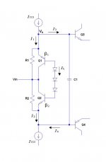
Here's my attempt to explain this bias circuit in a reasonably brief and simple way. The circuit is a little unusual. 
See diagram below. I have simplified SD's circuit by removing the input "diamond" buffer transistors because they are not needed to describe the behaviour. Also, I have explicitly shown the output resistances, R1 and R2, of the bias transistors (sometimes called hox; the Early effect). Typically, these are very large (tens of kohms) but when Vce is is very low they drop to very small values. This is because the current gain of the transistor, or beta, becomes very sensitive to changes in Vce.
Two, brief ways of describing the circuit operation:
1) Transconductance
Consider the upper half of the circuit. There is a current I1 flowing through Q1 (R1 is internal to Q1). There is a base current I3 flowing into the driver Q3. There is a CCS whose current must equal I1 + I3.
When Vin increases relative to Va, the Vce of Q1 decreases, and the current through R1 decreases, so I1 decreases. As I1 + I3 is constant, I3 must increase by the same amount. The transconductance is approximately 1/R1.
Note that R1 is non-linear...the smaller Q1 Vce is the smaller R1 is. R1 is like having a resistor in series with the driver's base...so it needs to be small enough to adequately tie Vin to Va. The nominal value of Vce is set by the diode chain.
2) Beta ratios and current flows
There is a relationship between I3 and I4 because the bases of Q1 and Q2 are connected together:
I4 = B2/B1.(I3 - Iccs) + Iccs
If B1 = B2 then I4 = I3. When Vin increases relative to Va, I3 increases and Q3 turns further on. B1 decreases because the Vce of Q1 decreases, and simultaneously B2 increases because Q2s Vce increases. The ratio B2/B1 increases and this causes I4 to decrease relative to I3, turning Q4 further off. It is possible in principle, if the beta ratio becomes large enough, for I4 to become negative, in which case Q4 turns off and the excess current flows into C1.
Hope this helps.
Sorry, but I can't really describe circuits accurately without using some maths.
Attachments
janneman said:What I meant was that whatever clever things the bias circuit does to track output currents or temp or what, in the end the bias is kept sort of constant by that cap between the driver bases, meaning the amp is definitely switching it's output devices on and off.
I agree with that, Jan.
robson fulco said:Hello good afternoon to all ...
I am a friend of carlos goosander and I am making the amp. Dunlap's got some doubts ..
which the value of the cap. C2 that this side of the transistor Q5?
not found in the same schema ...
grateful for the attention of all
Hi Robson - it's is good to see a friend of Carlos the Destroyer here!! Welcome!! 😀 😀 😀 Thank you for building this amplifier for Carlos while his health is not so good - you must be a very good friend to have!
I have asked Steve about this capacitor in the past - and it is very rare that it is used - most likely not required. It is used to stop high frequency oscillations if I remember what Steve told me. If it is required I am not sure what value it would be. Hopefully he will check in and give us some information. 😉
Hi Thomas,
-Chris
That gives us a very good idea what the part is and possibly the approximate value might be. Do you have a schematic, the one for the board? The cap is probably in parallel with a resistor. If you find the resistor on the PCB, you can identify where it is on the schematic and "pencil" it in on the schematic. The position of this capacitor may suggest a value for it.It is used to stop high frequency oscillations if I remember what Steve told me.
-Chris
ostripper said:
That much I know..but , I was talking about the 6 - to-126's.
Running at 8-10mA CCS, they are HOT!! It gets 40C here and
with that much heat, semi's don't last as long. I was thinking
of bolting all 6 to a 1" strip of aluminum flashing, at least.
OS
AND the answer is (envelope please)
I have not recommended heat sinks for the TO220 transistors. They should be dissipating 0.56W with the 56V supplies for the 100W amp. Only 0.36 for the 50W amp. They are rated to dissipate 2W at 25C ambient. The interior of the amp will run above ambient, but not hot enough to place a stress on the transistors. I use 40C for my sims. This does give results that differ from the standard 25C. Where I have mentioned heat sinks is for the pass transistors in the regulated supply. That is printed just to the right of those transistors on the schematic.
Steve
Hope this helps. Steve is a bit out of sorts today so I'm trying to help all I can. Some answers may be a bit lacking but I'm doing the best I can with what I have to work with.
Hi Thomas,
Gee, I wish I could have an amp running right now. All these questions could be cleared up with one running amplifier.
The temperature of these devices would be one of the things I would be looking at. They may be fine, maybe not for long term use.
I wonder, would the use of a heat sink throw things off as far as the operation of this amplifier is concerned? That's a question for Steve once he is feeling better. I'll bet that can change from morning to evening easily for him.
-Chris
robson fulco said:Hello good afternoon to all ...
I am a friend of carlos goosander and I am making the amp. Dunlap's got some doubts ..
which the value of the cap. C2 that this side of the transistor Q5?
not found in the same schema ...
grateful for the attention of all
This is what Steve wrote about it:
"You are correct about C2. I left a place for it if it was needed. The value would be 30pF or less. I never had a problem but this makes it easy to correct if there was one."
anatech said:Hi Thomas,
That gives us a very good idea what the part is and possibly the approximate value might be. Do you have a schematic, the one for the board? The cap is probably in parallel with a resistor. If you find the resistor on the PCB, you can identify where it is on the schematic and "pencil" it in on the schematic. The position of this capacitor may suggest a value for it.
-Chris
A reply from Da Man: C2 (if needed) 5 to 12pF. 🙂
It is there to prevent oscillations -
- Status
- Not open for further replies.
- Home
- Amplifiers
- Solid State
- Krill - The little amp that might...