you can get flatpack versions of just about any standard diode
so the models would be the same. I just ordered some with
the same specs as murs120. ($.03 apiece) 😀
os
so the models would be the same. I just ordered some with
the same specs as murs120. ($.03 apiece) 😀
os
Hugh,
Atached is other "configuration" of Krill OPS.
If we look Q2 and Q4 they looks like cascode of Q1 and Q3 ( besides the base of Q2 and Q4 are not fixed voltage as normal cascode configuration ). So, the base impedance of Q9 and Q10 works as loads from those cascodes. But the input this circuit is on the "load" from that.
Is it a inverted use of cascode?
Or I´m foolish ?
Ed
Attachments
That's a great idea OS - nice thermal contact and a bit of a thermal trap with the pcb board covering them shielding the diodes thermally!
scott wurcer said:
Hugh this is not my concern. Ground the input and force +-2.5A into the output. At 25mA bias this represents (at least) two decades of current modulation between N and P halves or ~+-120mV of movement in the output. I don't see the tanh() component of this reduced to 50ppm at only 5-6mV across the degeneration. Steve stated explicitly that the differential voltage across the bases of the output devices does not change. Cancelling the inherent Vbe vs. Ic transfer function with a current depending on three betas does not fly.
This can be done on pencil and paper no simulators needed.

And the "non-switching" crowd are still ignoring that 1uF capacitor.
Is the next area of consideration for improvement in the CCS? I presume this needs to be rock solid and highly resistant to PS fluctuations. Can this be improved - maybe this is one of Steve's next revelations?
Is the next area of consideration for improvement in the CCS?
LED/22u cap /150R Re... is what I "cobbed" together , there ,a
higher gain device (KSA1220/KSC2682) at the "R" gain group
will give 3X regulation. Bias gen/diodes and darlington gain
are the only critical factors where actual device selection
matters. Of course the diamond itself should be fast/low Cob/
High Hfe(KSA1381/KSC3503 -"Y" gain group).
OS
Well, a CCS is far better than a resistor for one. For two, the performance of a simple LED / Transistor may be good enough for this duty. With the configurations I've been working with since 2003 or 2004, I have been using a non-cascoded CCS. A red LED and transistor have very similar temperature coefficients. If you can mount them together, the temperatures will remain similar.
So while a better CCS can be constructed, it may or may not have any real effect on performance.
Hi Hugh,
Than you for going through the operation of this circuit. I'm sure it's really helped a lot of people out.
-Chris
So while a better CCS can be constructed, it may or may not have any real effect on performance.
Hi Hugh,
Than you for going through the operation of this circuit. I'm sure it's really helped a lot of people out.
-Chris
Thank you John.
Hi Ed,
The circuit certainly bears some resemblance to a cascode, since it is a couple of transistors one on top of the other. However signal is applied to Q9 base and taken from Q2 emitter; normally, in a cascode, we would take the signal from a collector. So strictly, it is not a cascode.
Therefore, for this reason, it is not used as a cascode, since there is no voltage gain here. It's used as a unity gain tracker.
The input circuit seen by V3 (from your revised diagram using 5200/1943 outputs) is very high, as it is dominated by the collector loads of Q2 and Q4, both very high, seen by the Q9 and Q10 emitters, multiplied by the betas of Q9 and Q10. In practice, a bias resistor would be connected between bases of Q9/Q10 to ground, to reference signal to earth. This resistor would principally set the Zin, and a good value would be around 33K.
I have been discussing this circuit with Terry Demol, an Australian living in Sydney, and he graciously pointed out that I have missed something in my explanation. There is another mechanism operating in this novel circuit which is responsible for accommodating the very large increase in Vbe which takes place as the output devices switch on hard. This increase will be from 0.6V at quiescent to about 1V at 8A, based on the curves. Clearly as one side of the OPS turns on hard, the diode bias string passes less current, and this means the voltage drop across it must DECREASE. Something peculiar is happening here, since to keep all output devices on, the voltage across the diode string must INCREASE with increasing drive.
The truth is, it's two processes. The first, already discussed in post #1070, is the fact that as one side of the OPS turns on, the driver bias current increases, robbing the diode bias string of current it receives from the CCS on the rail. That much has been explained. But this does not explain how the voltage increases between the emitters of Q2 and Q4, ensuring the inactive side remains on.
Since the CCS on both rails always source/sink a constant current, Kirchoff's Law holds that the current sums at a node must net zero. So if we have 11mA coming out of the CCS, and 1mA is passed to a driver base, then 10mA must pass to the Q2/Q9 and Q4/Q10 devices. So how does the voltage between the emitters (and hence the bases) of Q2 and Q4 increase when the output current starts to increase on signal peaks and troughs?
When Q2 and Q4 are driven close to saturation, and this voltage, Vce, influences operation. As the Vce on a transistor drops, a knee on the curve takes effect and the beta of the transistor drops precipitously, meaning that in this application Vce must change as collector current reduces. As a positive going signal rises higher, more and more current flows through the output devices, and less current flows through Q2.
Q2 has less current through it, but reacts by reducing its Vce, 'squeezing' more voltage at the collectors of Q2 and Q4 for the same voltage across the diode string. But reducing Vce rapidly drops transistor beta, resulting in a massive increase in bias current passing down the diode string. This increases voltage drop across the diode string (their dynamic resistance is high, around 300-400 ohms, and Q4 also adjusts its Vce so that it passes the same current as Q2, forcing the bias from the base of Q6 to rise, keeping the inactive output stage side always on.
So the voltage across the diode string does increase as each OP side alternately turns on hard, and this does put more voltage between the emitters of Q2 and Q4, which drives the driver bases.
The purpose of C1 is merely to slow this up and down cycling of potential difference so that transitions are kept relatively relaxed and smooth, reducing distortion.
Thanks Terry, this is very interesting!! No doubt about it, this is a complicated circuit, with a very low component count.
Cheers,
Hugh
AKSA said:The purpose of C1 is merely to slow this up and down cycling of potential difference so that transitions are kept relatively relaxed and smooth, reducing distortion.
LOL!
The change in Vbe is only half the problem.
5A load peak current (50W / 4R) will develop 1.1V (above the ~6mV with a 25mA bias current setting) across the 0.22 R emitter resistor passing the load current (which would have to be dynamically and quickly accounted for by the bias generator to prevent the opposing darlington's Vbe from being reverse biased).
Any large cap between the driver bases defeates such a function and there is nothing "smooth" about the resultant switching at higher audio frequencies (assuming, for the sake of the argument, the bias generator performs as advertised without the capacitor).
EDDELARUE,
Seemingly, you`re not. Of course it`s not a cascode, which by definition is composed of a transconductance amplifier, where the output current is proportional to the input voltage, and of a current buffer, where the current is transferred unchanged. The question is, what is unchanged and what is proportional to what here? In other words, how linear is this arrangement?Or I´m foolish ?
Thanks Hugh, fantastic explanation 🙂
It's seems to be definitely to difficult for LTSpice 😎
Just as well Steve didn't have those tools back then, otherwise it may not have happened 😀
🙂
It's seems to be definitely to difficult for LTSpice 😎
Just as well Steve didn't have those tools back then, otherwise it may not have happened 😀
🙂
AKSA said:Thank you John.
Hi Ed,
The circuit certainly bears some resemblance to a cascode, since it is a couple of transistors one on top of the other. However signal is applied to Q9 base and taken from Q2 emitter; normally, in a cascode, we would take the signal from a collector. So strictly, it is not a cascode.
Therefore, for this reason, it is not used as a cascode, since there is no voltage gain here. It's used as a unity gain tracker.
The input circuit seen by V3 (from your revised diagram using 5200/1943 outputs) is very high, as it is dominated by the collector loads of Q2 and Q4, both very high, seen by the Q9 and Q10 emitters, multiplied by the betas of Q9 and Q10. In practice, a bias resistor would be connected between bases of Q9/Q10 to ground, to reference signal to earth. This resistor would principally set the Zin, and a good value would be around 33K.
I have been discussing this circuit with Terry Demol, an Australian living in Sydney, and he graciously pointed out that I have missed something in my explanation. There is another mechanism operating in this novel circuit which is responsible for accommodating the very large increase in Vbe which takes place as the output devices switch on hard. This increase will be from 0.6V at quiescent to about 1V at 8A, based on the curves. Clearly as one side of the OPS turns on hard, the diode bias string passes less current, and this means the voltage drop across it must DECREASE. Something peculiar is happening here, since to keep all output devices on, the voltage across the diode string must INCREASE with increasing drive.
The truth is, it's two processes. The first, already discussed in post #1070, is the fact that as one side of the OPS turns on, the driver bias current increases, robbing the diode bias string of current it receives from the CCS on the rail. That much has been explained. But this does not explain how the voltage increases between the emitters of Q2 and Q4, ensuring the inactive side remains on.
Since the CCS on both rails always source/sink a constant current, Kirchoff's Law holds that the current sums at a node must net zero. So if we have 11mA coming out of the CCS, and 1mA is passed to a driver base, then 10mA must pass to the Q2/Q9 and Q4/Q10 devices. So how does the voltage between the emitters (and hence the bases) of Q2 and Q4 increase when the output current starts to increase on signal peaks and troughs?
When Q2 and Q4 are driven close to saturation, and this voltage, Vce, influences operation. As the Vce on a transistor drops, a knee on the curve takes effect and the beta of the transistor drops precipitously, meaning that in this application Vce must change as collector current reduces. As a positive going signal rises higher, more and more current flows through the output devices, and less current flows through Q2.
Q2 has less current through it, but reacts by reducing its Vce, 'squeezing' more voltage at the collectors of Q2 and Q4 for the same voltage across the diode string. But reducing Vce rapidly drops transistor beta, resulting in a massive increase in bias current passing down the diode string. This increases voltage drop across the diode string (their dynamic resistance is high, around 300-400 ohms, and Q4 also adjusts its Vce so that it passes the same current as Q2, forcing the bias from the base of Q6 to rise, keeping the inactive output stage side always on.
So the voltage across the diode string does increase as each OP side alternately turns on hard, and this does put more voltage between the emitters of Q2 and Q4, which drives the driver bases.
The purpose of C1 is merely to slow this up and down cycling of potential difference so that transitions are kept relatively relaxed and smooth, reducing distortion.
Thanks Terry, this is very interesting!! No doubt about it, this is a complicated circuit, with a very low component count.
Cheers,
Hugh
Hello Hugh,
Thanks for the explanations. An intriguing circuit at the least. I can follow you as far as that 1uF cap. That really spoils it again AFAICS. You had a believeable explanation why, in the end, it would be possible for the bias to increase even if on the face of it it looked like it would decrease. But the Vbe of the drivers and output devices must follow in rithm with the signal, faithfully tracing every signal excursion, and that 1uF works against that by trying to keep those Vbe's constant. In other words, the 1uF almost makes sure that the devices DO switch off.
If there is an absolute need for that cap, it must be a reason and logic we haven't discovered yet...
Has anybody build this amp yet?
Jan Didden
janneman said:In other words, the 1uF almost makes sure that the devices DO switch off.
Actually it just makes sure (under certain conditions) that the Vbe of the Darlington opposing the one passing the load current is reverse biased. For some bizarre reason some people around here seem to refuse calling an output stage "switching" if there is a few hundred uA of cross-conduction at higher frequencies.

Cheers,
Glen
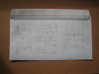
I think this circuit functions basically as a triple EF.
Here is a rough equivalent? circuit. It looks to me like all the
extra machinery is for Vbe multiplier/thermal compensation
(Q9/Q10 and associated circuitry).
Not criticizing, just trying to understand it. I'm also
wondering what role the CS's play in this, because they
aren't really needed in this equivalent? circuit.
Mike
Attachments
Maybe "switching less" than others...and this is already an advantage we can listen
....really if electrons spins clockwise or counter clockwise may be something interesting to some folks to study.... but.... spinning this way or that way..sounds good..and this is what should interest us.
regards,
Carlos
............................................................................................
While i am healing a friend is building.
An externally hosted image should be here but it was not working when we last tested it.
An externally hosted image should be here but it was not working when we last tested it.
Ah Carlos, trying to understand how the circuit works is also valuable as long as it is done in a non-confrontational manner as most here are now engaged in.
It allows us to further our understanding of the art & perhaps improve or adapt it to other circuits. Some balance has now emerged on this thread between explanation of the circuit & operation of the circuit although it seems likely that there are still more details to come out about it's workings!
I agree though that if it gets down to the quantum level explanation for it's operation my credulity will be stretched unless it turns out to be the worst option except for all the others as Churchill once said about democracy
Well... it is interesting too to understand deeply
and i gone as deepest as i could... i have simulated and found it do not switches into the simulator while low frequency is entering...
Having higher frequencies and that condenser....yes.... it may switch.
Enjoy folks.....my main enjoyment is to listen...but i see there are many ways to enjoy audio.... just be happy.
This is what matters...to enjoy and be happy.
regards,
Carlos

- Status
- Not open for further replies.
- Home
- Amplifiers
- Solid State
- Krill - The little amp that might...