jkeny said:SD stated that there was a definite null point which could be found using a distortion analyser but without this then set to 25mA as a useful set point but not necessarily the null point.
I think that was what got people going in the first place, at 25mA the simple Vbe vs Ic nonlinearity precludes those distortion numbers. Giving benefit of the doubt examining weather the nearly saturated devices caused an unexpected cancellation was necessary.
The funny thing is anyone with a decent scope could take a finished amp and find the effect, if any, by measuring a few nodes and thinking about it. There isn't much there I can't imagine it being more than an hour or so of work. A null could even involve actual build, grounding, bypass, signal routing, coupling, etc.
scott wurcer said:
I think that was what got people going in the first place, at 25mA the simple Vbe vs Ic nonlinearity precludes those distortion numbers. Giving benefit of the doubt examining weather the nearly saturated devices caused an unexpected cancellation was necessary.
The funny thing is anyone with a decent scope could take a finished amp and find the effect, if any, by measuring a few nodes and thinking about it. There isn't much there I can't imagine it being more than an hour or so of work. A null could even involve actual build, grounding, bypass, signal routing, coupling, etc.
The 25mA figure was suggested for the 50W amp if there was no access to equipment to measure the distortion null. I did not at any time state what bias the 400W amp was running.
Re: Mine is this one..... and this sample was not built...i have only an old version
Yes I will ! I´m very curious about that sound.
Thanks and congratulations to you and to Steve Dunlap for one more " toy " !
regards
Ed
destroyer X said:
Nice amplifier..... i suggest you to try Ed.
Yes I will ! I´m very curious about that sound.
Thanks and congratulations to you and to Steve Dunlap for one more " toy " !
regards
Ed
I assume you mean.
This stuff isn't Toys,
It's cultural shifts
2 cents +arrogance
regards
Max
This stuff isn't Toys,
It's cultural shifts
2 cents +arrogance
regards
Max
Member
Joined 2009
Paid Member
Pardon Me....
It's a long thread to wade through. I've spent some time on many pages but not much closer to deciding anything. Can we have a summary for new arrivals like me - I just want to figure out some basic things like "is the Krill amplifier a good choice for me?", "how much would it cost to build one and how easy are the parts to obtain", "why would I pick this over alternatives, even compared with a gainclone". If there's a FAQ or something for these rather basic questions please forgive my barging in...
It's a long thread to wade through. I've spent some time on many pages but not much closer to deciding anything. Can we have a summary for new arrivals like me - I just want to figure out some basic things like "is the Krill amplifier a good choice for me?", "how much would it cost to build one and how easy are the parts to obtain", "why would I pick this over alternatives, even compared with a gainclone". If there's a FAQ or something for these rather basic questions please forgive my barging in...
Post 809 has the BOM for all the parts.
Go to Mouser and Digi-key to see if you can afford it.
Go to Mouser and Digi-key to see if you can afford it.
Hi Bigun,
This amplifier output section has been reviewed twice in this thread and is thought to be well worth building. The older semiconductors may be cross referenced in a bit. I am not sure if the exact voltage amp stage Steve used has been posted yet.
I am hoping to build one at some point, it looks intriguing and the base design is known to have great detail.
For now, I think we should investigate the circuit idea and Steve's exact design as we go along.
Hi Steve,
Welcome, it is an unexpected pleasure to see you post. Thank you.
-Chris
Juma,
This is the one I'm talking about - don't know what post but it's shown for the 200W version & could be applied to all versions, I presume. Firstly it replaces the offset trimmers with LDRs and the rest of the additional circuitry is the output DC sensing & dynamic adjustment of the LDRs to maintain an DC offset of zero.
Edit: Welcome back Steve, I hope this next phase of the thread is more enjoyable for you than what has transpired 'til now?
Attachments
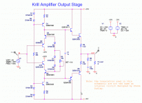
There's been a lot of confusion about how Steve's circuit works. I've run this by him, and he's OKed this description which relies on the attached basic schematic:
1. Input goes positive, lifting base of Q9, and with it, the emitter of Q9.
2. As emitter Q9 rises, it eventually starts to saturate Q2, but Q2 is passing a constant current from the CCS at Q1, so it CANNOT turn off. Fortunately, both the base and the emitter of Q2 are not set at a fixed voltage, so that to accommodate current flow from the CCS, they can actually move up and down in voltage under drive from the emitter of Q2 without constraint.
3. So, as Q9 emitter moves up, Q2 responds by moving up with it since emitter and base are not controlled or fixed. But as Q9 moves up, the voltage across Q2 (Vce) starts to reduce, close to saturation.
4. As Q9 emitter moves higher, it turns on harder the driver (Q5) and its associated output device (Q7). The base current required by the driver rapidly starts to rise. This means LESS current passes to the emitter of Q2. In turn, this means LESS base bias needs to be drawn from the base of Q2 to maintain current through it, and so less bias current flows down the bias string.
5. With less current drawn from the base of Q2, less current must now pass to the base of Q4, since any current entering the bias diode string can only be injected into the base of Q4. So Q4 MUST pass less current as well since its bias is reduced. In fact, the current passed by Q2 is pretty much the same as that passed by Q4; this is a direct result of the shared base bias of Q2 and Q4.
6. With Q4 now passing less current, any shortfall must be drawn from the base of Q6 since the CCS sinks a constant current. The voltage at Q4's emitter will slightly adjust to keep Q6 on, however, so even with the positive side of the amp passing many amps, the negative side will still stay on.
The complementary mechanism applies for negative input swings so that the output stage devices, all of them, will ALWAYS remain on. A question remains, however, how do we set the minimum and maximum currents in the inactive side whilst keeping a reasonably low quiescent? I suspect it's just device choice, very important to have the right diodes and transistors.
This is a highly creative circuit, but it is subtle and unusual, because the drive passes through a collector, not the usual base or emitter. It's a tricky topology to understand, and this has led to many different interpretations, not least a diversity of simulated distortion profiles. The criticism of the designer is to be expected; people generally deride what they cannot understand.
Hats off, Steve!
Hugh
Attachments
Thanks Hugh,
Great explanation!
I think I understand this in my simplistic way, so two questions occur to me
- conceptually what conditions determine the null point?
- Ostripper is correct that the diode string & Bias transistors are intimately connected - again what is the condition necessary for deciding this combination - the current range in the diode string between max pos swing & max neg swing of input signal?
AKSA said:... I suspect it's just device choice, very important to have the right diodes and transistors.
This is a highly creative circuit, but it is subtle and unusual, because the drive passes through a collector, not the usual base or emitter. It's a tricky topology to understand, and this has led to many different interpretations, not least a diversity of simulated distortion profiles. The criticism of the designer is to be expected; people generally deride what they cannot understand.
Hats off, Steve!
Hugh
Yes, absolutely correct 🙂😎
PS: Thank you Hugh for taking the time to liaise with Steve (very much appreciated) and welcome back Steve (very much appreciated) 🙂😎
Hi John,
- conceptually what conditions determine the null point?
If by null point, you mean idle condition, where no signal is passing, then this is simply the voltage across the diode string, and the resulting voltage between the emitters of Q2 and Q4. This takes account of the saturation voltage of these transistors, the Vce, since this must also add to the voltage across the diode string.
It is the bias voltage from emitter Q2 to emitter Q4 which determines the quiescent current of the output stage. Typically this is 2.40 volts.
- Ostripper is correct that the diode string & Bias transistors are intimately connected - again what is the condition necessary for deciding this combination - the current range in the diode string between max pos swing & max neg swing of input signal?
I cannot tell you this with any accuracy, as simulations are not particularly reliable with LTSpice, and I've not built and measured the circuit. You'd need to measure it on a working example. However, a little calculation could reveal the ballpark; both CCSs are set to approx 11mA, and for output device quiescent of 50mA, beta of 80 and driver beta of 100, the driver bias at quiescent would be around 50/80*100 = 0.00625mA, or 6.25uA, a tiny percentage (0.057%) of the CCS current.
This would mean that nominally 99.943% of the CCS current flows into Q2/Q4 in the quiescent state.
As we ramp up the output stage, say the positive side, to 2A (2000mA), the bias draw at the driver increases to 0.25mA - and probably a bit more because with increasing output current the output device beta tends to drop slightly. Let's assume 0.3mA. So now only 10.7mA flows to Q2, and this reduces base bias from say 11/150 = 0.073mA (based on beta 150 for Q2 and Q4) to 10.7/150 = 0.071mA. This reduced bias is fed to Q4, too, of course, and results in less current passed through it and a bit more passed to the driver Q6.
If the output stage were passing 7A, let's say, and beta of the output device dropped to 60, we would have a bias requirement at the driver of 7000/60*100 = 1.167mA, assuming driver beta does not drop. This is subtracted from the 11mA of the CCS to give us 9.833mA through Q2, reducing its bias requirement from 73uA to 65.5uA. This is not much, and easily unbalanced if the diode strings and Q2/Q4 suffer wandering temperature. Steve runs his Q2/Q4 at higher temperatures with minimal heatsinking to eliminate the effects of variations in ambient; a very good idea.
As alluded to earlier, the disadvantage of this clever scheme is the susceptibility to temperature effects; I've not built it, so can't comment further, but it would, I think, be very sensitive to temperature changes at Q2/Q4 and the diode string. The outputs substantially drop Vbe with increasing temperature, so quiescent control would need to be fine tuned by placing one or more of the diodes onto the heatsink. A fair bit of experimentation would be necessary to get this right; I think Steve has it nailed, but operation in very cold climates might be problematic since there is a greater range of temperatures from switch on to full output.
Hope this helps,
Cheers,
Hugh
- conceptually what conditions determine the null point?
- conceptually what conditions determine the null point?
If by null point, you mean idle condition, where no signal is passing, then this is simply the voltage across the diode string, and the resulting voltage between the emitters of Q2 and Q4. This takes account of the saturation voltage of these transistors, the Vce, since this must also add to the voltage across the diode string.
It is the bias voltage from emitter Q2 to emitter Q4 which determines the quiescent current of the output stage. Typically this is 2.40 volts.
- Ostripper is correct that the diode string & Bias transistors are intimately connected - again what is the condition necessary for deciding this combination - the current range in the diode string between max pos swing & max neg swing of input signal?
I cannot tell you this with any accuracy, as simulations are not particularly reliable with LTSpice, and I've not built and measured the circuit. You'd need to measure it on a working example. However, a little calculation could reveal the ballpark; both CCSs are set to approx 11mA, and for output device quiescent of 50mA, beta of 80 and driver beta of 100, the driver bias at quiescent would be around 50/80*100 = 0.00625mA, or 6.25uA, a tiny percentage (0.057%) of the CCS current.
This would mean that nominally 99.943% of the CCS current flows into Q2/Q4 in the quiescent state.
As we ramp up the output stage, say the positive side, to 2A (2000mA), the bias draw at the driver increases to 0.25mA - and probably a bit more because with increasing output current the output device beta tends to drop slightly. Let's assume 0.3mA. So now only 10.7mA flows to Q2, and this reduces base bias from say 11/150 = 0.073mA (based on beta 150 for Q2 and Q4) to 10.7/150 = 0.071mA. This reduced bias is fed to Q4, too, of course, and results in less current passed through it and a bit more passed to the driver Q6.
If the output stage were passing 7A, let's say, and beta of the output device dropped to 60, we would have a bias requirement at the driver of 7000/60*100 = 1.167mA, assuming driver beta does not drop. This is subtracted from the 11mA of the CCS to give us 9.833mA through Q2, reducing its bias requirement from 73uA to 65.5uA. This is not much, and easily unbalanced if the diode strings and Q2/Q4 suffer wandering temperature. Steve runs his Q2/Q4 at higher temperatures with minimal heatsinking to eliminate the effects of variations in ambient; a very good idea.
As alluded to earlier, the disadvantage of this clever scheme is the susceptibility to temperature effects; I've not built it, so can't comment further, but it would, I think, be very sensitive to temperature changes at Q2/Q4 and the diode string. The outputs substantially drop Vbe with increasing temperature, so quiescent control would need to be fine tuned by placing one or more of the diodes onto the heatsink. A fair bit of experimentation would be necessary to get this right; I think Steve has it nailed, but operation in very cold climates might be problematic since there is a greater range of temperatures from switch on to full output.
Hope this helps,
Cheers,
Hugh
- conceptually what conditions determine the null point?
Thanks again Hugh
Your gentle, calm manner brings a needed air of quietude to this thread! Much appreciate your learned, exemplary & generous approach to this circuit.
What I actually meant by the "null point" was the null point of THD that Steve had alluded to. But no need to answer this as I suspect it's only ascertained by measurement.
I might be wrong but was it mentioned earlier in the thread about the concept of using something like some BD139s as the diode string & therefore being able to bolt them onto to heatsink for better thermal tracking/stability?
Edit: I found my answer here: quote:
Originally posted by lumanauw
Hi, Steve,
In earlier page, you mentioned about using Q7,8,10,11 for thermal compensation by attaching those to heatsink.
Is this better/worse than attaching the bias diodes in the heatsink?
The tracking is pretty much the same either way. Just slightly faster with the diodes because of their lower thermal mass.
I chose to put the diodes on the heat sink because I didn't want to buy a larger heat sink to accommodate 4 more transistors. The diodes only require one hole for mounting and can be placed very close to the outputs at the center of the heat sink.
I would have also needed to make the board wider to move those transistors to the edge for mounting to the heat sink.
AKSA said:Hi John,
- conceptually what conditions determine the null point?
Hope this helps,
Cheers,
Hugh
- conceptually what conditions determine the null point?
Hugh this is not my concern. Ground the input and force +-2.5A into the output. At 25mA bias this represents (at least) two decades of current modulation between N and P halves or ~+-120mV of movement in the output. I don't see the tanh() component of this reduced to 50ppm at only 5-6mV across the degeneration. Steve stated explicitly that the differential voltage across the bases of the output devices does not change. Cancelling the inherent Vbe vs. Ic transfer function with a current depending on three betas does not fly.
This can be done on pencil and paper no simulators needed.
scott wurcer said:This can be done on pencil and paper no simulators needed.
Don't fool yourself. For most, pencil and paper is way more complicated than handling a simulator.
Steve - it's great to see you looking in on things - hopefully to be encouraged to wade deeper into the pool.
We have a couple of mod's watching over things so the choppy waters should calm down to a manageable level. With over 53,000 views on this thread you have to "feel da luv" that the vast majority of us have for your and your design.
Hugh - thank you very much for taking the time to communicate with Steve and punch out a short version of the theory of operation. After my 5 way by-pass a year ago I tend to shy away from theory and anything that has the word operation attached to it. Very nicely done Sir!! I love the Aussie attitude of "cut the cra(x)" let's get something done here! 😀 😀 😀
BTW - the painters will finish up tomorrow and I hope to resume my construction of a pair of 50W mono-block's this weekend. Steve - get the test gear warmed up - I'll be heading over there in a few days. 😉
Attached - photo of home office this morning. The good news is that it was painted today. The bad news is that I'm using my safe as a chair to sit on while I'm working on the computer.
We have a couple of mod's watching over things so the choppy waters should calm down to a manageable level. With over 53,000 views on this thread you have to "feel da luv" that the vast majority of us have for your and your design.
Hugh - thank you very much for taking the time to communicate with Steve and punch out a short version of the theory of operation. After my 5 way by-pass a year ago I tend to shy away from theory and anything that has the word operation attached to it.
Very nicely done Sir!! I love the Aussie attitude of "cut the cra(x)" let's get something done here! 😀 😀 😀BTW - the painters will finish up tomorrow and I hope to resume my construction of a pair of 50W mono-block's this weekend. Steve - get the test gear warmed up - I'll be heading over there in a few days. 😉
Attached - photo of home office this morning. The good news is that it was painted today. The bad news is that I'm using my safe as a chair to sit on while I'm working on the computer.
Attachments

Some background about incredible Steves Amplifiers
Just a little things we all should know about Steve's amplifiers:
http://www.soundstage.com/masz02.htm
We all should respect Mr. Steve's wish to show us the way
to the better and more pleasant sound at our listening experiences to anyone who actually wish to build his excellent sounding AMPLIFIER and enjoy the good sound
He did to all of us - UNSELFISH -
Many, many THNX for Your's contribution to this forum dear STEVE.
I wish You all my congrats about Yours truly great Soul and Spirit.
Andrew
By jkeny -I might be wrong but was it mentioned earlier in the thread about the concept of using something like some BD139s as the diode string & therefore being able to bolt them onto to heatsink for better thermal tracking/stability?
Try 4(3) SMD "flatpack" diodes carefully soldered to a 1 X 1 pcb
with a screw in the middle. This is the standard for all my amps now.
I'm glad to see Hugh so elegantly explain the mechanism of
operation. (Uh oh ,he said it "does not switch off") 😀

OS
- Status
- Not open for further replies.
- Home
- Amplifiers
- Solid State
- Krill - The little amp that might...