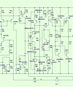
Because of diamond buffer output stage?
Q001 has wrong base-collector connection.
Q003+Q713 makes the right side diamond, Q711+(Q720//Q722//R734) makes left side diamond, R732(with help of C725 bootstrapp) makes the diamond CCS.
Steve, is it sufficient to use only R+bootstrapp (R732, R733=8k2 + C725=10uF) for powering an output diamond buffer, instead of using CCS like your version?
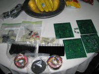
I drove over to Steve's today and let him bleed my wallet of a few $$$ for parts to build his Krill monoblock's.
Two amplifiers are for me and two are for ................. (the envelope - please) ........... Andypairo from Milano
😎
No - the bowl of banana's was not included in the price.
Two amplifiers are for me and two are for ................. (the envelope - please) ........... Andypairo from Milano
😎
No - the bowl of banana's was not included in the price.
Attachments
Ragnwald said:
Hi Steve
For sure lots of people is reading and learning out of this thread on daily base. 🙂
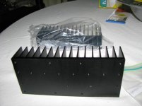
Please Steve, show us your skills in machining. Did you also make your own heat sinks?
PS. When you attach someones answer to your reply, make a mark in the little white square in the right corner (Quote).
I did not make the heat sinks shown in the photos earlier in the thread. These were made by Thermalloy from drawings I provided. It would be a lot of work to machine 250 heat sinks!
The intent was not to show my skills as a machinist, but rather to show how to build nice looking cases at affordable prices. Very few tools are needed. The amp shown here is one of my first cases built this way (actually the first 25 were built this way) and cost me $25 in Aluminum (each). The Al was pre cut to size when I bought it. With over 20 years of experience building my own, I now do a better job. This was before I studied machining and I didn't own a machine shop at the time.
http://www.diyaudio.com/forums/showthread.php?postid=1685711#post1685711
I did make the heat sinks in this amp but they don't show in this picture.
Zen Mod said:Steve - this thread gets 16200 hits ;
it seems that's some interest ........
but generally - sometimes lack of comments is just proof that things are sorta clear 😉
Thanks. I does seem that interest is picking up.
I know I'm slow responding but that's just because I'm slow. I have some catching up to do now and I will try to answer in the order the posts were made.
m2003br said:Hi Steve, Thanks for share your very interesting design.
I will make a try very sooner.
But, as you asked for errors on schematic, I did find a missing connection between the node of two zeners to ground, in Power supply schematic. (both 50 and 100W versions)
Regards,
Marcos
You are correct. The corrected 50W schematic is attached. I will attach the corrected 100W schematic on the next post.
Attachments
ostripper said:
That is right, what I would like to know is how the current
stage is thermally compensated.
It might be a dumb question but I could find no reference
to it in the thread.
It looks like that has been answered, but just in case you want to hear it from me, here goes.
The three diodes on the very small diode board are for thermal compensation. This board is mounted to the heat sink near the output transistors. You can see the location in the photo in post 323. It is the mounting hole below the row for mounting the outputs and drivers, just below the center of the heat sink.
Here is the corrected 100W schematic.
Attachments
jkeny said:Hi Steve,
Just another correction - the boards you sent out have C3 & C4 which isn't on the schematic sent with the boards - I believe these Cs are correctly shown on your recently posted 100W schematic.
Also, early in the thread you mentioned you would be post high power schematic (which you've done, thanks) & circuit improvements. Are there any other suggested circuit improvements besides the DC offset R30&R31 bypassed with pots ?(on the latest 100W schematic)
C3 and C4 are local decoupling caps for the VGA power supply. They were inadvertently left off the 50W schematic. I will make that correction tomorrow.
Since you are using a tube VGA and not the one on the board you would not add these caps.
jkeny said:OStripper is correct - in the stuffing guide there is a daughter card with a Q, R, D C component - this is beside the 3 diodes you refer to MJL. The actual boards only come with a small daughter board for the 3 diodes which act as thermal bias correction. So maybe the other components were also related to this function? Steve will clarify, I'm sure
Those parts were on another board that never got made or used. They are only on the stuffing guide because the only copy I could find after all these years was a paper copy. I have changed computers three times since I did these files originally and I am not sure where they are anymore. If I find them (probably in storage somewhere) I will delete these parts from the stuffing guide and post better artwork for the stuffing and boards.
Hi, steve I,m glad your back.. Lumanlauw was right , i saw the
diamond on the marantz and it triggered the brain.
As I am porting any useful topologies for my own greedy use
these days, let's see if I have it "reckoned".
Q7/10 are the diamond buffer, Q8/11 are just a diode biased
VBE ,Q9/12 are current sources used for the current stage to
improve psrr to counter the lack of global NFB, and 13-16
are very high gain darlington pairs (carlos doesn't like darlingtons
,by the way 😀 ).
I really like the topology and what it does for the Op stage,
By looking at the marantz , anything (VAS/input wise)
can be the source..😎 I am playing with the NFB factor
now, comparing how irt reacts with different VAS's and
NFB configs.
lumanauw said:Because of diamond buffer output stage?
Q001 has wrong base-collector connection.
Q003+Q713 makes the right side diamond, Q711+(Q720//Q722//R734) makes left side diamond, R732(with help of C725 bootstrapp) makes the diamond CCS.
Steve, is it sufficient to use only R+bootstrapp (R732, R733=8k2 + C725=10uF) for powering an output diamond buffer, instead of using CCS like your version?
Sorry, I still don't see it. At least to me, this does not resemble my output stage. It is biased differently, thermal tracking is different and I really don't believe a resistor is an acceptable replacement for a current source. I believe that also answers your question about the CCS.
I don't believe Q001 is the only mistake in that schematic.
c2cthomas said:The heat-sinks that Steve has are very nice and pre-drilled! That will save the cost of a couple of drill bits!!
Pre drilled AND pre tapped. The holes have 4-40 threads.
By steve D.- this does not resemble my output stage.
No, not exactly , but they are both diamond based. I agree,
that with real CCS's, performance is MUCH better. I used
a Standard Vbe (for ease of construction) and lowered the
darlingtons gain slightly (more of a high gain EF instead)
because of oscillations with fast devices at saturation.
Because the krill/diamond stage presents almost no load on the
vas , i could run at 2-3mA..😎 which might allow for
faster SMD or to-92 devices.
OS
Attachments
ostripper said:Hi, steve I,m glad your back.. Lumanlauw was right , i saw the
diamond on the marantz and it triggered the brain.
As I am porting any useful topologies for my own greedy use
these days, let's see if I have it "reckoned".
Q7/10 are the diamond buffer, Q8/11 are just a diode biased
VBE ,Q9/12 are current sources used for the current stage to
improve psrr to counter the lack of global NFB, and 13-16
are very high gain darlington pairs (carlos doesn't like darlingtons
,by the way 😀 ).
I really like the topology and what it does for the Op stage,
By looking at the marantz , anything (VAS/input wise)
can be the source..😎 I am playing with the NFB factor
now, comparing how irt reacts with different VAS's and
NFB configs.
The Marantz was not the only amp to use what people these days are calling a diamond buffer and certainly not the first. If Q7/Q10 are what you are calling a diamond buffer then this is a really old configuration going back at least 35 years. That is when I first saw it. I have no idea how long before that.
There are good reasons for its use as an input stage. First, you can DC couple. Second, it gives .6V on the emitter of Q7 and -.6V on the emitter of Q10. This gives you bias for the next power stage so it has an idle current. Understand that I am describing the circuit as I first saw it but using the schematic designations from my schematic to make this easier to follow. In the original that would on been Q13/Q15. Their emitters would have been tied to the load through emitter resistors. Drive for the Q13/Q15 was supplied by the current sources of Q9/Q12. Q7/Q10 sink all current that does not flow in the bases of Q13/Q15. The emitters of Q7/Q10 follow the base connection allowing the current sources to track the emitters up and down swings and Q13/Q15 are emitter followers. This makes a simple 6 transistor buffer that is reasonably well behaved. This was my starting point.
The drawback to this is the amount of heat generated by the current sources for higher output power such as an amplifier. All the base current for outputs is from the current sources. With the power transistors available 35 years ago the gain was usually low so the current sources needed to supply .5A to 1A to achieve reasonable output power. With 50V or higher rails this made for some serious heat - 200 to 300W at idle.
Another drawback was the fact that the only way to adjust output bias was by changing the value of the emitter resistors.
I addressed the first problem by using a Darlington output. This greatly reduced the heat in the current sources as now they could be run at 50mA or less. This then required me to provide a second .6V drop for each output. I didn't like using a diode or resistor because I did not feel they were the optimum solution. The solution was to repeat the input pair to give the additional .6V drop. I then added the diodes and trim resistor so the output bias could be adjusted over a wide range. Placing the diodes on the heat sink gave thermal compensation. This solution also had the benefit of having the only source of base current for either Q8/Q11being the base of the other. When one output Darlington (say Q13/Q14) draws base current from its current source (Q9) then less current flows in Q7. This reduces the current flowing in the bases of both Q7 and Q10. This makes less base current available to Q10 causing Q10 to try to turn off. This increases the resistance of Q10 which increases the base voltage of the other output Darlington causing it to stay in conduction during more or even all of the output voltage swing.
Proper output bias is set using a distortion meter and observing the sharp null in distortion as you reach the optimum.
Does this help understand the circuit?
No more tonight. I actually sleep occasionally.
We need to be real teachers to be so good as you are Dunlap
there are many teachers, or masters that repeats book paragraphs alike parrots repeating something they have listened... sometimes i understand they know things but they do not want you to know too... they confuse, do not explain...show themselves under the spot and cooperate nothing with forum progress... those non real teachers drives me mad.... sometimes i felt the need to jump inside the screen to travell into space to hold their necks with my strong fingers and make them spit their tongue, for some moments, to show their behavior not aproved...not acceptable, at least to me and some other more cooperative folks.
Teacher is you!... the real one!.... the one motivates us to follow your schematic and to be happy with that 0.6 volts ready to go to the next stage... the real understanding...the real description... the step by step, the logic sequence...... "this happened because this one have happened first... and will trigger this, that and those as consequences!"
You see... since 35 years ago, or more...people posting "diamond buffer"...people designing the circuit and i could never understand by myself just watching...had an idea of course..but there were gaps on that understanding... something remaining not understood.... and i am sure...alike me hundreds are having the chance to understand deeply because of you... the real cooperative behavior... a real helping hand.
Your contribution is memorised for whole life in my brain, and you had offered me the "key" to understand much more circuits.
Teacher....yeah!.... teacher!.... a real one.... designers!... well.... thousands can do that...but to be good teacher..only few guys can do that.
Congratulations Dear Steve Dunlap.... i want to let you know that one day i will have the pleasure to have a dinner... a nice Italian Pizza with you.
An externally hosted image should be here but it was not working when we last tested it.
An externally hosted image should be here but it was not working when we last tested it.
Zen Mod said:
I know , but I must tease ya 😉
Ko ce koga ako ne svoj svoga ! 😀
You are fully entitled to it !
😉
Re: We need to be real teachers to be so good as you are Dunlap
destroyer X said:... those non real teachers drives me mad.... sometimes i felt the need to jump inside the screen to travell into space to hold their necks with my strong fingers and make them spit their tongue, for some moments, to show their behavior not aproved...not acceptable,
jkeny said:Hi Steve,
Just another correction - the boards you sent out have C3 & C4 which isn't on the schematic sent with the boards - I believe these Cs are correctly shown on your recently posted 100W schematic.
Also, early in the thread you mentioned you would be post high power schematic (which you've done, thanks) & circuit improvements. Are there any other suggested circuit improvements besides the DC offset R30&R31 bypassed with pots ?(on the latest 100W schematic)
Yes there are other improvements. I will get to those eventually. I'm still waiting for someone to build one of the simple 50W amps and report back. Subjective sound is very much a matter of personal taste. It is possible that people will not prefer the sound of this amp, but I find that unlikely.
- Status
- Not open for further replies.
- Home
- Amplifiers
- Solid State
- Krill - The little amp that might...